New family of components emerge from arrayed waveguide gratings

Designers are using AWGs to create a variety of components, raising the possibility of integrating complex functions into a single monolithic chip, interconnected by waveguides.
The arrayed waveguide grating (AWG) is a planar waveguide device that functions like a transmissive diffraction grating in bulk optics, diffracting light at angles that depend on the wavelength. Initially, it was developed mostly for wavelength-division multiplexing (WDM) and demultiplexing. Although WDM remains the primary application for arrayed waveguide gratings, developers have found that AWGs can be integrated with other planar waveguide components for a variety of other functions, including dynamic gain equalization, reconfigurable optical add/drop multiplexers, and wavelength-selectable lasers.
Basic principles
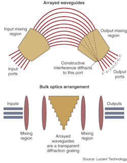
The arrayed waveguide grating consists of an array of narrow waveguides running beside each other between a pair of mixing regions or coupling zones. Input signals enter the first mixing region where they are coupled into several curved waveguides running to the second mixing region (see Fig. 1). These waveguides differ in length by an increment ΔL, which is much larger than a wavelength and corresponds to a phase delay of nΔL/λ, where n is the refractive index of the waveguide.
The light transmitted by the waveguides interacts as it enters the second mixing region, where diffraction spreads wavelengths at different angles, like a diffraction grating. The mixing region acts like a lens to focus the diffracted light onto a series of output ports on the opposite side. Constructive interference focuses light of a particular wavelength at only one point on the opposite side, with the ports arranged to collect light at the desired wavelength ranges, such as standard optical channel slots for WDM. The number of output ports is the number of channels separated, with the free spectral range of the device equaling the channel spacing multiplied by the number of channels. The number of waveguides running between the two mixing regions is greater than the number of channels; for example, a 64-channel waveguide AWG has an array of 232 waveguides linking the mixing regions.
One can think of an AWG as a planar-waveguide implementation of high-order transmission grating (see Fig. 1 bottom). Arrayed waveguides can be fabricated in silica, plastic, silicon, or III-V semiconductor such as indium phosphide. As a planar waveguide device, it can be fabricated monolithically and integrated with other components. Both features are important. Although a master AWG is expensive, its cost does not increase dramatically with the number of wavelengths handled, making it attractive for high-port-count WDM. Once the master has been produced, the unit cost drops sharply. Integration also makes it possible to combine AWGs with optical switches and other components to perform complex functions.
The design imposes some inherent limitations on AWGs. Insertion losses are relatively large, arising from mode mismatches between the waveguides and the mixing regions, although tapering the waveguides can reduce this mismatch. Small phase errors in the arrayed waveguides and the excitation of high-order modes in the waveguides produce some interchannel crosstalk.
Polarization and temperature dependence are significant issues. Polarization sensitivity is largest in III-V semiconductor waveguides, arising from the inherent birefringence of the material. It is less in silica, and lowest in silicon waveguides fabricated on insulators. A variety of approaches have been developed to reduce these sensitivities.
Like other optical waveguide devices, AWGs are larger than integrated electronic circuits because more room is needed to bend light. Increasing the refractive-index increment between the waveguide and the substrate from 0.65% to more than 1.5% can reduce the required bend radius from 6 to 8 mm to about 2 mm in a super-high-delta waveguide. However, increasing the waveguide index leads to higher fiber-coupling losses.
Multiplexers/demultiplexers
Arrayed waveguide gratings have gained acceptance for WDM with high channel counts because their integration allows lower cost per channel than systems based on discrete optics. Laboratory versions have achieved extremely high channel counts and spacings, with channel spacing to 10 GHz and hundreds of channels in a single device.1 Typical commercial devices have channel counts of about 40. The best-known application for AWGs is for demultiplexing, with a single input carrying a WDM signal that is demultiplexed so the optical channels are separated among many output waveguides. For multiplexing, the device can be reversed, with signals at separate wavelengths entering separate ports and being combined inside the AWG.
Standard AWGs have passbands that are nearly Gaussian in shape, so they strongly attenuate light from adjacent passbands. However, the ideal passband for WDM has a flat top rather than the curved Gaussian peak. The simplest approach to flattening the peak is spatial filtering by adjusting the way light is delivered to the input port, or by adjusting the lengths of the array arms. One alternative is to add an interleaver to split signals between a pair of AWGs, one receiving the odd channels, the other the even channels. Another approach is to add a second AWG or another waveguide component for additional filtering.
Wavelength routing relies on the same principles as the AWG demultiplexer. As with other gratings, the diffraction angle of the arrayed waveguide depends on the angle of incidence as well as the geometry of the grating. If all the optical channels enter through a single fiber, they all have the same angle of incidence. However, if light enters the input mixer through two or more input ports, those inputs have different incidence angles, so they are diffracted at different angles as they emerge from the arrayed waveguides in the output mixer. This effect can be used to reroute and rearrange optical channels carried by multiple input fibers. The routing pattern is fixed, but the passive device ensures that channels with the same wavelength won't interfere with each other or be routed out the same waveguide.
Tunable filtering
Arrayed waveguides can serve as the basis for a family of integrated tunable components. The basic idea is to use a pair of AWGs back-to-back to separate and then recombine optical channels (see Fig. 2). The channels can be processed separately between the demultiplexing and remultiplexing stages. The type of processing depends on the application.

This approach has been taken in making dynamic gain-equalization filters. Conceptually, the simplest approach is to insert a variable optical attenuator in each waveguide channel carrying a separate wavelength between the two AWGs. Tuning these variable attenuators can compensate for gain variations between channels, but it introduces extra loss into a system that is already lossy. An alternative is to split the optical signal before putting one part of it through the back-to-back waveguides.2 Instead of putting variable optical attenuators on each channel, this design uses phase-shifters that shift the phase of the light passing through the AWG pair relative to the light bypassing them. The phase shift can attenuate the selected channels when the two composite signals are recombined; with less total loss than if variable optical attenuators were used. Note that in this case the waveguide lengths must be matched so all channels pass through the combined device without any unintended phase shift, so the lengths must be the same. By using a different approach, AWGs could provide tunable dispersion compensation.
The back-to-back AWG design can be extended further to make a reconfigurable optical add/drop multiplexer. In this case, the first AWG demultiplexes the through input signal and delivers the separated optical channels to an array of optical switches. Channels to be added locally are delivered to the switch array by a separate set of waveguides. The switches then direct the signals they receive to one of two AWG multiplexers—one collecting signals for the drop, the other collecting signals for through transmission. Such switching techniques can be extended for other applications, such as wavelength-selective crossconnects.
Semiconductor AWGs can be integrated with active devices to provide other functions. Monolithic integration can combine indium phosphide detectors with AWGs both for use in receivers and for signal monitoring; devices have been demonstrated in several laboratories. Integration of semiconductor optical amplifiers between demultiplexing and multiplexing AWGs can compensate for large optical losses. Semiconductor amplifiers or electroabsorption modulators can be installed as switches.
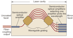
Semiconductor optical amplifiers can be combined with AWGs to make multichannel semiconductor lasers. Forty-channel devices have been demonstrated in the laboratory and several approaches are being investigated.
Outlook and overview
Arrayed waveguide devices are complex, and much work remains on practical issues such as attenuation, and sensitivity to temperature and polarization. Developers are working to make attenuation uniform across the entire operating range, and to shape passbands to better meet application requirements. Design tools are being developed to extend the range of AWG applications. Although current AWGs are small by optical standards, they are large and costly compared to integrated electronic chips.
Yet AWGs have the promise of meeting one of the long-held goals of optical communications: the ability to integrate complex functions into a single monolithic chip, interconnected by waveguides. If the economies of scale can be realized, these sophisticated components could be mass-produced at low cost, like their electronic counterparts, opening new possibilities for optics.
REFERENCES
- K. Takada et al., IEEE Photon. Tech. Lett. 13, 1182(2001).
- C. Doerr et al., IEEE Photon. Tech. Lett.11, 581 (1999).
FURTHER READING
For an overview of current research, see J. Capmany et al., editors, special issue on Arrayed Grating Routers/WDM Mux Demuxs and related applications/Uses, IEEE J. Select. Topics Quant. Electron. 8 (November/December 2002).
Christopher Doerr, Tutorial TuV1, OFC 2003.