Mask makers contemplate the next generation
This year's SPIE symposium on photomask technology, held in September in Monterey, CA, opened with descriptions of deep-UV (DUV) laser writers replacing electron-beam (e-beam) systems and closed with discussions of maskless lithography. The opening technical presentation, a joint paper by Cypress Semiconductors (San Jose, CA) and DuPont Photomasks (Round Rock, TX), compared mask and wafer results for a 90-nm-node Metal 1 layer, written from three mask-writing platforms (50 keV e-beam, a DUV laser, and a 365-nm laser). Based on the competitive DUV performance, an effort to convert all four of the 50-keV 90-nm-node vector-scan beam layers to the DUV writer is under way at Cypress.
Expanding on the idea of moving away from 50-keV vector-scan tools to low-cost ownership of laser writers, Paul Allen of Etec Systems, an Applied Materials (Santa Clara, CA) company, followed with a description of aerial-image-enhancement improvement on the company's DUV laser writer, which uses pixel-level operations performed with software in the geometrical data—rather than at the mask optical proximity compensation (OPC) level—to significantly improve pattern fidelity. Perceived barriers in transitioning to laser writers have been primarily that the entire OPC libraries must be recomputed to account for differences in pattern fidelity, and also that differences in pattern fidelity may affect system yield, he said.
"But the [DUV laser writer] is already in production and serving multiple sites for 130- and 90-nm design rules and those existing systems are already producing comparable results to 50-keV systems," he said. The aerial-image-enhancement improvement is expected to further address these concerns by causing the delivered mask pattern to more closely represent the input pattern data, with improved corner acuity, reduced corner pull-back, and reduced line-end shortening. The improvements were demonstrated by using software in the geometry engines of the laser-writer system, which slowed down write times, but Allen said that Etec is about to install the enhancement algorithms into the field-programmable gate arrays that perform gray-level mapping—an approach that will result in no delay in write times.
Curt Jackson of DuPont Photomasks (Round Rock, TX) followed Allen's talk with a discussion of chemically amplified resists for DUV printing of photomasks and showed comparable results to 50-keV vector-scan beam mask writing by the Micronic (Täby, Sweden) system as well as Etec's system.
Mask design specifications
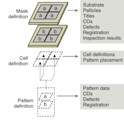
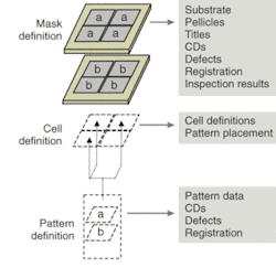
Other mask-related efficiency items discussed at the meeting included the significance to mask makers—in both process efficiency and yield—of the role of communicating mask design specifications. "The number one reason for a mask being bad is errors in the front end," said John Duff, a regional manager for Molecular Imprints (Austin, TX), who also taught a short course on Photomask fabrication and technology basics. He advocated use of the "SEMI P10" file standard for automated information transfer as a means of enabling the mask maker to process design and mask-preparation information more rapidly and accurately. A poster presentation by Michael Behnam of Agilent Technologies (Palo Alto, CA) and Jim McCracken of CenterLink (San Jose, CA) sounded a similar theme: "More than 40% of photomask returns are due to job-planning and front-end administration errors." Agilent upgraded its photomask order-management software with a personal-computer-based version for photomask order management that produces SEMI P10 output, with positive results. "One photomask vendor reports average front-end cycle time with SEMI P10 has been reduced by one to two hours with a 20% reduction in order errors," say the authors (see figure).
A plenary session on maskless lithography was motivated by statistics such as 43% of masks are rejected for functional errors. The session included a wide range of perspectives, and several speakers from Micronic and ASML (Veldoven, The Netherlands) discussed their ambitious joint program to produce an optical maskless lithography system that would begin shipping by the end of 2006.
Bert Jan Kampherbeek described efforts at startup Mapper Lithography (Delft, The Netherlands) to develop a maskless lithography system based on a combination of massively parallel electron-beam lithography (more than 13,000 beams) along with MEMS and telecom technology, with a goal of a full-system demo by the fourth quarter of 2004.
Dave Adler of KLA-Tencor (San Jose, CA) put the whole session and perhaps the whole week-long symposium in perspective, however, in describing the task requirements of direct-write inspection: "If a single chip was the size of North America, it would be like inspecting every pothole in North America in an hour."

