Ion milling makes diamond micro-optics
Diamond optics transmit over a large spectral range, conduct heat very well, resist etching, and are exceedingly hard. These same properties, however, make fabricating diamond optics difficult—standard methods of micromachining are either inefficient or stressful enough to crack diamond films. Yongqi Fu at the Nanyang Technological University (Singapore) and others may have found a way around this problem by milling the films with focused beams of gallium (Ga) ions.1 The researchers used the process to make a diffractive optical element (DOE) and found that neither the transmission nor index of refraction was altered much, while the efficiency of the DOE was sufficient for practical use.
Other groups have used photolithography and plasma etching to mill diamond coatings (see Laser Focus World, April 2003, p. 26). The advantage of the focused-ion-milling method is that it offers one-step direct fabrication on the film, according to Fu. Also, the room-temperature method is localized so one area can be altered without any effect on other areas of the film. "It is very useful for microfabrication of planar micro-optical devices," says Fu.
The group is interested in machining microcrystalline diamond-like coatings. Because internal stresses cause diamond films to delaminate when they are thicker than about 2 µm, the group is looking at diffractive optical elements (DOEs) that typically have a design depth of 1 µm, rather than thicker refractive optical elements. The group used continuous vapor deposition to grow a 1.5-µm-thick film on a fused-silica substrate, which contained both sp3 (diamond) bonds and sp2 (graphite) bonds between the carbon atoms.
The machining process is a direct-writing method called focused-ion-beam milling. The researchers used a focused-ion-beam machine integrated with a scanning electron microscope, with liquid Ga as the ion source. The machine produces a focused Ga+ ion beam with an energy of 50 keV, a probe current ranging from 4 pA to 19.7 nA, and a 25- to 350-µm beam-limiting aperture. At the lowest currents, the beam can be focused down to 7 nm in diameter. Varying the ion dose changes the milling depth.
Properties change—a little
The higher the proportion of sp3 bonds in the film, the closer the index of refraction and transmission spectrum resembles crystalline diamond. The researchers noted that the proportion of diamond bonds to graphite bonds was higher in the film before milling than afterward. They believe that the Ga-ion bombardment causes some of the bonds to convert to sp2.
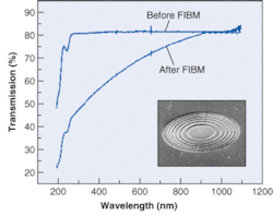
The milling also caused a decrease in transmission in the visible, and to a lesser extent in the near-infrared up to about 900 nm. The refractive index increases after milling. In the near-IR, the refractive index is about 2.2 (other IR materials, such as germanium, gallium arsenide, and indium phosphide, have refractive indices of around 3 or 4). They note that designs for diamond DOEs made by this process should use the post-milling refractive index. "It should be easier," Fu's group writes, "to realize achromats if the substrate of the DOE is an infrared material." By and large, however, the optical changes caused by the room-temperature milling process do not preclude conventional use.
To show that the process is usable, they fabricated a DOE on the film (see figure). The researchers found that the accuracy of the surface relief depended on the beam spot size and the amount of overlap during raster scanning. Larger-sized beams and lower overlaps resulted in less-exact relief features. They were able to control the depth of milling more accurately than lateral errors.
The element took about 20 minutes to fabricate. This is too slow for mass production, but can either be used for prototyping microdevices or for creating a master that could be used for making replicas in a different material.
When used with a 1550-nm laser, the DOE proved to be about 73% efficient, which is sufficient for practical use. "For conventional use," Fu says, "diffraction efficiencies above 60% are okay."
REFERENCE
- Yongqi Fu et al., Rev. Scientific Instruments 74(8) (August 2003).

