Native-nitride passivation eliminates facet failure

Now more than 40 years old, laser-diode technology has become critical for photonics, underpinning applications from data storage and solid-state industrial lasers to telecommunications. Despite its maturity, this technology still faces reliability and longevity issues in certain high-power applications, most notably in pumping Nd:YVO4 (vanadate) and Nd:YAG lasers. In this case, the main problem is oxidation of the exposed facet, which leads to absorption and ultimately device failure resulting from catastrophic optical mirror damage (COMD). Several approaches have been used to address this problem, mainly involving protective passivation coating. But to date, none of these methods has proved completely satisfactory at 806 nm.
A novel approach has been developed that directly seals the dangling surface bonds and eliminates susceptibility to oxidation and subsequent device failure. Unlike other approaches, this method is broadly applicable to all types of III-V semiconductor lasers from blue-emitting diodes to those operating in the 1550-nm telecommunications region.
Surface oxidation and COMD
Most laser diodes are III-V edge-emitting devices. Typically, their structures are created on a single wafer, which is then cleaved to separate the individual lasers and expose the facets. One end of the device becomes the output facet and is coated with an antireflection coating. A multilayer high-reflection coating is applied to the opposite facet. In addition to their optical purpose, these coatings also protect the facets from oxidation.
After cleaving, the exposed surface is chemically highly reactive because atoms in the surface layer are not fully bonded and possess what are commonly called "dangling bonds." If this surface comes into contact with air or moisture, oxidation rapidly occurs. When the device is powered up, the oxidation products absorb the laser light and heat the facet. Moreover, the oxides appear to have catalytic properties leading to material breakdown deeper and deeper into the laser crystal. Ultimately, laser fluence and increasing absorption result in device failure due to COMD at the output facet. In fact, without protective optical coatings, most edge-emitting laser diodes would fail within seconds of being powered up.
Despite this problem, longer-wavelength and lower-power devices have been developed that deliver many years of reliable operation, typically through the use of various so-called passivation techniques. The most commonly used methods involve coating the freshly exposed facet with a thin (on the order of 30 Å) layer of silicon (Si) or zinc selenide to seal the surface. The optical coatings are then applied over this passivation layer. Typically, the entire cleaving and passivation process must be performed under ultrahigh vacuum (UHV) to reduce the possibility of surface oxidation prior to passivation. This step adds complexity and cost and reduces productivity.
High-power 806-nm laser diodes
Pumping solid-state Nd:YAG and Nd:YVO4 lasers requires a laser-diode output closely matched to the absorption of the laser medium, typically in the 805- to 808-nm range. The laser-diode wavelength is determined by the composition and design of its quantum well. For high-power operation at 806 nm, there are two main material systems that are used today: aluminum indium gallium arsenide (AlInGaAs), and indium gallium arsenide phosphide (InGaAsP).
Through the addition of In to the quantum well, AlInGaAs overcomes notorious dark-line defects and related degradation found in traditional AlGaAs devices. The benefit of In comes at the price of increased Al concentration—from 5% for AlGaAs to 15% for AlInGaAs. Unfortunately, the greater the proportion of Al, the bigger the oxidation problem and the greater the need for effective facet protection. But Si passivation of AlInGaAs diodes at 806 nm has been very problematic at this short wavelength for several reasons. First, the Si layer efficiently absorbs laser light at 806 nm, thereby heating the facet. In addition, Si can actually migrate into the laser diode, causing more absorption. Also, facet-surface imperfections and the thinness of the Si layer mean that some oxygen and/or water will find their way to the Al and cause oxidation. This can even happen during subsequent deposition of the antireflection and high-reflection coatings applied to the facets, which typically contain alumina layers at 806 nm. As a result, Si-based passivation only retards rather than prevents facet oxidation and COMD in Al-containing laser diodes.
More recently, InGaAsP materials have shown reduced susceptibility to COMD. Unfortunately, the output power of InGaAsP lasers is much more temperature-sensitive than that of AlInGaAs lasers, so, high-power InGaAsP lasers must be very efficiently cooled, usually by bonding to a water-cooled copper heat sink. Moreover, very dissimilar thermal expansion coefficients of InGaAsP and copper require direct bonding of laser bars with soft In metal (for strain relief and efficient heat transfer) to sustain high-power operation. This can be an acceptable arrangement for continuous operation, but most real-world applications require repeated on/off cycling of the diode or diode-pumped laser. Ultimately, this slowly tears the softer In layer, leading to loss of thermal conduction and long-term device failure.
In contrast, AlInGaAs can be bonded to an expansion-matched copper/tungsten submount using hard (gold/tin) solder, which is then attached to a copper heat sink, again with hard solder. Thus, AlInGaAs would clearly be the best material for long-lived high-power operation, providing the oxidation issue could be successfully eliminated.
Atomic sealing via the N2-IBE process
Milling with argon- or nitrogen-ion beams was originally investigated as early as 20 years ago by several teams, including Carsten Lindström and colleagues at Xerox PARC (Palo Alto, CA). It was considered as a surface smoothing and cleaning tool for removing contaminants, such as oxides, from the facet surface. If conditions are properly adjusted, however, the nitrogen ions produce an even more important effect: they actually bond with the exposed group III atoms on the surface, terminating the dangling bonds as chemically stable nitrides.
This is the basis of the native-nitride ion-beam epitaxy (N2-IBE) process, which was recently refined and perfected at Comlase and has patents pending. Specifically, four critical process variables have been optimized: the ion-beam energy, the ion-beam density, the exposure time, and the composition of the background gas mixture. Now, in a single process, the oxides are removed from the surface, the surface is smoothed, and the exposed, pristine III-V surface is chemically stabilized by saturating the dangling bonds. Even if this surface is subsequently exposed to air or moisture or coated with oxide-based thin-film coatings, there are no activated group-III atoms available to be oxidized.
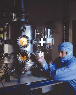
Another result is productivity and cost effectiveness; unlike some of the traditional passivation techniques, the N2-IBE process eliminates the need to cleave the dies under UHV, since the process cleans the surface and seals the dangling bonds at the same time. Without the need for critical alignment or capital-intensive UHV cleaving systems, the N2-IBE process cost-effectively delivers very high throughput and yield; moreover, the optical coatings can be produced in the same load-locked vacuum chamber used for the N2-IBE process, reducing laser-diode handling, production complexity, and cycle time (see Fig. 1).
The resultant native surface nitrides have high stability and, because of their high bandgaps, do not absorb at any laser-diode emission wavelengths. For example, AlN has a bandgap of 6.2 eV, GaN of 3.3 eV, and InN of greater than 2.0 eV; thus these nitrides have no discernible optical effect.
Testing shows low degradation
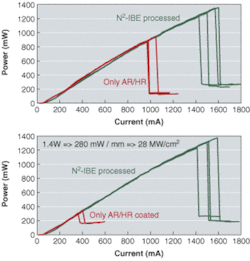
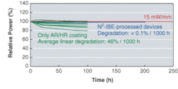
Testing of samples of single-mode AlInGaAs devices at 806 nm validates this process. Pulsed testing has shown that N2-IBE raises COMD threshold before operation by an average of 45% (see Fig. 2). The median COMD value increases to 1.3 W, which corresponds to a COMD value of more than 30 W for 100-µm-wide emitters. Moreover, after screening at 15-mW/µm power densities, N2-IBE-processed devices remain unchanged at a median COMD of 1.3 W while the COMD of standard coated devices decreases by 64%. In terms of device lifetimes, aging tests at 15 mW/µm indicate an extremely low power degradation of less than 0.1%/1000 h for N2-IBE-processed lasers compared to an average of 46%/1000 h for standard coated lasers (see Fig. 3). Based on this success at 806 nm, we are planning to extend the N2-IBE process to 937 nm for disk-laser pumping, 915 nm for fiber lasers, and to lasers emitting at less than 700 nm.
The N2-IBE process is highly compatible with existing semiconductor-production methodologies, and can boost productivity and lower cost compared to alternative technologies. The process works over an extremely wide range of materials systems and wavelengths, including gallium nitride at 404 nm, AlInGaP at less than 700 nm, AlInGaAs, InGaAsP and InGaAs for 750 to 980 nm, and InP at 1700 nm. High-power single-mode InGaAs lasers at 980 nm, processed with N2-IBE, recently passed Telcordia qualification with a projected median lifetime of 75 years.
CHRISTOFER SILFVENIUS is process engineering manager, PETER BLIXT is vice president of commerce and business development, CARSTEN LINDSTRÖM is vice president of operations and chief technology officer, and ALFRED FEITISCH is president and chief executive officer at Comlase AB, SE, 126 75, Stockholm, Sweden, and Los Gatos, CA; e-mail: [email protected].