Pulsed lasers micromachine photonic integrated circuits
ARZU M. OZKAN-ANDERSON
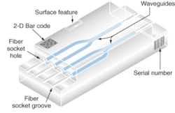
Optoelectronic modules serve many existing and emerging applications including telecommunications, data storage, and the "lab-on-a-chip" biosensors used for biological threat detection or in point-of-care diagnostic systems. Many of these optoelectronic (OE) devices can now be made as monolithic glass modules because of new, pulsed-laser micromachining technologies that allow efficient all-laser fabrication as well as offering certain performance advantages. Several steps are involved, including singulation of the glass modules, marking them with unique identifiers, and the creation of subsurface features such as optical waveguides and Bragg gratings. Micromachining of external features—such as fiber socket holes and grooves—is also necessary so that light can be coupled into and out of these modules (see Fig. 1).
Singulation and marking
The process of cutting and separating large glass sheets into smaller individual glass substrates is called singulation and traditionally has been carried out using a mechanical scribe-and-break method. A diamond blade scribes the glass before it is mechanically broken along the scribed lines. However, in industries in which singulation is common—such as the fabrication of flat-panel displays—250- to 500-W sealed carbon dioxide (CO2) lasers are now used to cut glass at a rate of up to 300 mm/s.1 Unlike the mechanical method, laser cutting does not create microcracks that can propagate over time within the glass substrate. Furthermore, laser cutting has the potential to increase overall yield and productivity by eliminating most of the post-process polishing and cleaning necessary to smooth rough edges and by eliminating the glass dust that would otherwise be created during scribing.
After singulation and before any subsequent processing, each glass substrate typically is marked with a unique serial number or a logo to help identify and track the module through the manufacturing process. The nanosecond-pulse output of an ultraviolet (UV) diode-pumped solid-state (DPSS) laser at either 355 or 266 nm (depending on glass type) marks the glass modules. When a UV laser beam is focused inside the glass volume, a controlled microcrack is formed. Computer-controlled scanning mirrors translate the focal spot to create highly visible alphanumeric characters within the glass (see Fig. 2).
Writing gratings and waveguides
Bragg gratings are often used in optical communications for wavelength selection and gain modification.2 The gratings are typically produced by direct write with a continuous-wave (CW) or nanosecond-pulse UV laser that creates a regular index of refraction change in the glass.3 This technique has several limitations, however. The UV-induced change in the index of refraction in many types of glass is small and tends to alter with time and temperature, which severely limits the choice of glasses from which Bragg gratings can be made. Moreover, UV penetration depth is small in most glasses, thereby preventing this technique from producing three-dimensional subsurface structures.
Standard waveguide-manufacturing methods like physical vapor deposition and ionic exchange are also restricted to the glass surface, which means that multiple waveguide layers cannot be created within the volume of a glass module using these techniques. Micromachining with femtosecond pulses can overcome these limitations.4
Ultrafast femtosecond pulses deposit laser energy into the electrons of materials in much less time than the transfer time of this energy to the bulk of the material. There is, therefore, negligible energy deposition to the surrounding material, either by electron-phonon coupling or by thermal diffusion, and any energy transfer to the bulk material is limited to a small volume.
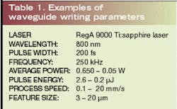
Unlike UV lasers, ultrafast lasers are able to perform subsurface modifications to the index of refraction of many glass materials because the interaction is wavelength independent. The energy of tightly focused femtosecond pulses is absorbed in a focal volume via multiphoton and avalanche ionization.5, 6 Because subsurface heating, melting, and resolidification are confined to a small volume by the surrounding material, three-dimensional spatial restructuring can be performed to create Bragg gratings, as well as closely spaced three-dimensional waveguides for planar lightwave chips and other integrated optics. Bragg gratings and waveguides have been created by ultrafast lasers in various glasses, including fused silica, BK7, and soda lime. A range of parameters for waveguide writing is shown in Table 1.
Bulk surface machining
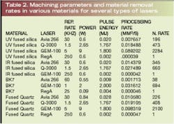
External features machined out of the glass surface are required in the fabrication of the OE modules so that fibers can couple light into the optical circuits.7 Recent studies have compared material processing rates to determine the best material and laser combinations for machining surface features (see Table 2).
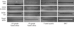
Although optimizing processing speed is the primary goal, the quality of a machined feature must also be considered when determining the best laser for machining (see Fig. 3). Ultraviolet processing at 266 nm causes poor results in both fused silica and quartz, with chipping of material and irregular, poorly defined wall geometry. This is because of the low absorption (<10%) of fused silica at 266 nm. The UV light is first absorbed by surface imperfections and impurities that damage the surface and increase the number of absorbing defect sites. These sites are heated further by subsequent UV photons. This heating eventually leads to catastrophic material breakdown and ablation. The extreme chipping and fracturing around groove walls in fused silica and quartz indicate forceful material ejection by escaping plasma. In contrast, 266-nm light is very well absorbed by BK7, and UV laser machining of this material yields excellent results.
Infrared processing of fused silica and quartz in the nanosecond-pulse-width regime (using a Q-switched CO2 laser) yields grooves with well-defined edge qualities and high material removal rates. However, it is difficult to achieve tight machining tolerances (±5 µm) with CO2 lasers, because of their long wavelength, which yields spot sizes between 50 to 100 µm. Although IR processing in the microsecond regime (with the GEM-100) offers the highest material removal rates, the interaction is highly thermal and causes melting of the sidewalls. This occurs because low-frequency IR light is strongly absorbed by glass atoms and molecules. In the case of BK7, both the GEM-100 and GEM Q-3000 instantly crack the material, because of the material's low thermal shock resistance.
Femtosecond machining of fused silica, quartz, and BK7 is precise and occurs through multiphoton absorption. Because material removal is limited to the immediate vicinity of the focal volume, ultrafine, micron-by-micron machining can be carried out in layers. Furthermore, a 5-µm spot size allows both a tight bend-radius around corners and tight geometrical tolerances. Although femtosecond lasers offer the advantages of ultrafine precision for material removal and a minimal heat-affected zone (HAZ), they are only efficient for machining features that are less than 10 µm in size. When feature sizes increase to the range of hundreds of microns to a few millimeters, femtosecond processing becomes too slow and, therefore, too expensive.
REFERENCES
- S. Lee, Information Display 17(3) 20 (March 2001)
- K. O. Hill, Y. Fuji, D. J. Johnson, and B. S. Kawasaki, Appl. Phys. Lett. 32, 647 (1978).
- G. Meltz, W. W. Morey, and W. H. Glenn, Opt. Lett. 14, 823 (1989).
- A. M. Ozkan and L. Migliore, SPIE Proc. 4978 162 (2003).
- A. M. Ozkan et al. "The Third Pacific Rim Intl. Conf. Adv. Materials and Processin (PRICM 3) Proc., sponsored by the Minerals, Metals and Materials Society, Honolulu, Hawaii (July 1998).
- A. M. Ozkan, A.P. Malshe, T.A. Railkar, and W.D. Brown, Appl. Phys. Lett. 75, 3719 (1999).
- T. Hoult, A. Ozkan, L. Migliore, and T. Corboline, Nepcon West Fiber Optic Conf. Proc., FA4B.
Arzu M. Ozkan-Anderson is a senior laser applications engineer at Coherent, 5100 Patrick Henry Dr., Santa Clara, CA 95054; e-mail: [email protected].
