PHOTONIC CRYSTALS: Photons flow in liquid circuits

FRANCESCA INTONTI, SILVIA VIGNOLINI, MARCELLO COLOCCI, AND DIEDERIK S. WIERSMA
Photonic crystals offer promise as a substrate for all-optical devices that may eventually circumvent the intrinsic miniaturization limits of silicon-based integrated electronic circuits.
Photonic-crystal systems are characterized by a periodic modulation of the refractive index that can be achieved, for example, by perforating a solid medium with a periodic array of air holes. The light traveling in this ordered array of scatterers undergoes refractions and internal reflections that, because of interference effects, substantially influence the propagation of light.
If the refractive-index gradient is steep enough along certain directions, the interference can be destructive for the propagation of light with a wavelength comparable to the spatial periodicity of the refractive-index modulation or lattice constant of the photonic crystal. A photonic crystal can therefore act as a “light insulator” and the wavelength range within which light cannot propagate inside the crystal is called the photonic bandgap, analogous to the electronic bandgap for electrons in semiconductors. In fact, the periodic modulation of the refractive index acts on photons in much the same way as the atomic lattice potential does on electrons in semiconductors.
Continuing with the solid-state analogy, consider the substitution of an atom in the crystalline lattice of a semiconductor with an atom from a different group, enabling the formation of a permitted state in the electronic bandgap. Similarly, a defect in an otherwise perfect photonic crystal can lead to localized photonic states in the gap, whose properties would depend on the shape and geometry of the defect. A point defect could act as a microcavity and a line defect as a waveguide.1
Connecting functional designs
Based on the idea of intentionally introducing crystal defects, a broad range of potentially functional designs, such as integrated microcavities, channel drop filters, optical switches, and low-threshold lasers have been proposed. Connecting such devices could essentially enable the photonic version of an integrated electronic circuit. Traditionally, the experimental realization of such structures is technically very difficult and limited to simple photonic-crystal design variations, such as missing pores, pores of different sizes, and/or pores at different positions, all of which must be incorporated at the growth stage of the photonic crystal.
An alternative and much more flexible approach for functionalizing 2-D photonic crystals consists of locally filling single pores of the crystal with liquids.2 If the refractive index of the filling material is sufficiently close to that of the surrounding matrix, the filled pore behaves the same as a missing pore, except that the defect can be erased and overwritten.
The infiltrated liquid can be easily removed by dipping the photonic crystal in an ultrasonic bath, opening the way to rewritable circuits and reconfigurable integrated photonic-circuit chips. Alternatively, using polymer composites enables the creation of permanent structures.
The ability to address a single pore also allows creation of local light sources by filling pores with active materials, such as colloidal quantum dots, in solution. In one of our designs, the photons created by optically pumping the colloidal quantum dots are guided through the sample along a waveguide, obtained by infiltrating adjacent pores in a linear geometry, until they reach a Y-shaped intersection (see Fig. 1). Here, depending on the alignment of the liquid crystals infiltrated in the lower branch (blue), the photons propagate either in the S-shaped branch or in both arms.3
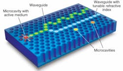
Two point-defect microcavities are placed along the tunable waveguide and can couple with the light flowing in the waveguide whenever the photon wavelength matches their resonances. The use of liquids with different refractive indices allows the design of cavities that couple light at different wavelengths and thus work as selective add/drop filters.
Nontrivial realization
Even if the concept of controlling the flow of light by filling the single pore of a 2-D photonic crystal is quite intuitive, the pore width and spacing must be of the same size as the wavelength of light (a few hundred nanometers). So, not surprisingly, experimental realization of this concept has not been at all trivial: the typical amount of liquid necessary to fill a pore is three orders of magnitude smaller than the liquid droplets ejected by sophisticated ink-jet printers.
Our realization of devices via controlled microinfiltration on a periodic two-dimensional macroporous silicon with honeycomb geometry4, 5 has been accomplished with a system that combines a microinfiltration setup (Eppendorf, FemtoJet) and three microscopes: a conventional optical microscope (Zeiss, Axioech), a confocal laser-scanning microscope (home built), and a scanning near-field microscope (Omicron, TwinSnom).
The conventional microscope monitors the approach of a micropipette on the sample surface. The tip of the micropipette is less than 1 µm wide, fixed to a positioning system that can locate the pipette tip with a lateral precision of 100 nm. When the tip is on the selected pore and the liquid meniscus is in contact with the sample, it is possible to fill the pore completely with the solution because capillary forces dominate the infiltration process. The filling liquid is a solution of water and fluorescent dye, allowing filled pores to be seen easily with a confocal laser-scanning microscope.
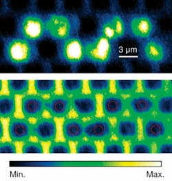
The use of this kind of microscope permits both improved spatial resolution and the collection of images of the same portion of the sample in reflection and fluorescence configuration. The reflection images offer a picture of the 2-D photonic structure, highlighting the pore positions, while the fluorescence images reveal the spatial distribution of the infiltrated material: the comparison of the two images represents a valid microinfiltration check. Images recorded with the confocal laser-scanning microscope illustrate successful realization of a sinuously bent waveguide obtained by sequential infiltration of a single pore of a 2-D photonic structure with an S-shaped geometry (see Fig. 2). The position of the light spots in Fig. 2, top, exactly corresponds to the air holes highlighted with red circles in Fig. 2, bottom, bearing out that the liquid has been introduced solely in the selected pores. Similar data have been collected using a solution containing liquid crystals, demonstrating the feasibility of externally tunable integrated devices.
Telecommunications window
Clearly, the most attractive range for application-based systems is the telecommunications window. Photonic crystals working with wavelengths on the order of 1.3 µm are characterized by a lattice constant of about 0.5 µm, which is below the resolution limit imposed by diffraction. Therefore, to push the microinfiltration method to a wavelength region of larger interest, the microscope must be able to see structures smaller than half a micron. The scanning near-field optical microscope fulfills this requirement because its spatial resolution is not diffraction limited, depending instead on the dimensions of the near-field probe.
During measurements, the near-field probe is closely rastered across the sample surface, at a constant distance of few nanometers, to provide sensitivity to the near-field signal. Therefore, the optical as well as the topographical image are simultaneously collected. In an infiltration experiment conducted to create an integrated local LED or laser source in a microcavity resonant at 1.3 µm, the cavity geometry consisted of a large pore with diameter of 700 nm that substituted for seven neighboring pores of a 2-D photonic crystal (see Fig. 3).
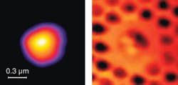
The crystal was fabricated by nanodrilling a pattern of holes with triangular symmetry into a silicon bulk sample. The active medium was a solution of lead sulfide (PbS) quantum dots characterized by a broad emission spectrum centered at 1.3 µm. Fig. 3, left, shows the topography image in which the cavity structure is clearly visible, and it is also possible to observe some material on the lower left side of the hole cavity, presumably related to the infiltrated quantum dots. The corresponding optical image, Fig. 3, right, shows that the signal distribution stems from the cavity center, confirming that the microinfiltration technique is a valid approach for functionalizing photonic-crystal structures designed for working in the telecommunication range.
Besides the increased flexibility of introducing defects of different types and natures that can be connected together in an all-optical circuit, the microinfiltration approach offers a post-fabrication method for exactly tuning the energy defect resonance by using a mixture of liquids of different refractive index. Beyond integrated optics, the technique can be applied for any local infiltration application, such as creation of sensor chips by locally infiltrating a liquid that changes its optical properties when exposed to different gases or biological species.❏
ACKNOWLEDGMENTS
The authors thank V. Türck for technical assistance with the CLSM and P. Bettotti, L. Pavesi, S.L. Schweizer, R. Wehrsphon, M. Bellotti, and Y. Chen for providing high-quality 2-D photonic-crystal samples infiltrated in this study.
REFERENCES
1. J.D. Joannopoulos, R.D. Meade, J.N. Winn, Photonic Crystals: Molding the flow of light, Princeton University Press (1995).
2. F. Intonti, S. Vignolini, V. Tuerck et al., Appl. Phys. Lett. 89, 211117 (2006).
3. H. Takeda, K. Yoshino, Phys. Rev. B 67, 73106 (2003).
4. A. Birner, R.B. Wehrspohn, U. Gösele, K. Busch, Adv. Mater. 13, 377 (2001).
5. P. Bettotti, L. Dal Negro, Z. Gaburro et al., J. Appl. Phys. 92, 6966 (2002).
Tell us what you think about this article. Send an e-mail to [email protected].
FRANCESCA INTONTI is a postdoctoral researcher, SILVIA VIGNOLINI is a Ph.D. student, MARCELLO COLOCCI is a full professor, and DIEDERIK WIERSMA is a group leader at the European Laboratory for Non-Linear Spectroscopy (LENS), Via Nello Carrara 1, 50019 Sesto Fiorentino (Florence), Italy; e-mail: [email protected]; www.lens.unifi.it.