PHOTOLITHOGRAPHY: Multiphoton technique creates 65 nm features with visible light
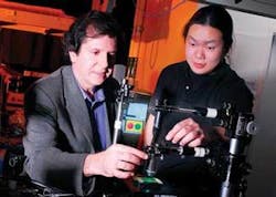
A Georgia Institute of Technology (Georgia Tech; Atlanta, GA) research team led by Joe Perry has developed a 3-D multiphoton-lithography technique that may provide a simpler and less expensive alternative to electron-beam (e-beam) and extreme-ultraviolet (EUV) lithography for fabricating many devices with nanoscale features. The technique scans 520 nm femtosecond-laser pulses across a polymer film containing a 4,4’-bis(di-n-butylamino)biphenyl (DAPB) chromophore to create structures in the polymer with linewidths smaller than the diffraction limit. So far, 3-D nanoscale features as small as 65 nm have been formed.
Maskless and low-cost
E-beam systems can provide linewidths of about 10 or 20 nm, but require multimillion-dollar equipment, whereas equipment for the multiphoton-lithography method proposed by Perry and colleagues is expected to cost about $700,000. Unlike the scanning approach of e-beam and multiphoton lithography, mask-based EUV lithography offers extremely high throughput for large-scale mass production. But, unlike multiphoton lithography, EUV systems require exotic optics that are also very expensive and difficult to maintain. Therefore, Perry expects his group’s approach to prove most competitive with existing approaches aimed at small to moderately large projects, particularly those that require creating batches of widely varying designs and specification. Because the multiphoton process is maskless, it is easy to reconfigure by computer.
Linewidths achievable with the multiphoton method are determined by the spatial distribution of light intensity at the beam focus, which creates crosslinks in the polymer material that harden the material and create the pattern that will remain after the film is washed in a solvent. The density of crosslinking at any point is proportional to the square of the beam intensity for two-photon absorption (or the cube for three-photon absorption) multiplied by the exposure time. In a Gaussian beam, for example, squaring the intensity reduces the spatial cross section near the peak by the square root of two. Thus, the ability to write subdiffraction linewidths is provided in part by sharpening the excitation profile to reduce the spatial profile.
A second mechanism for obtaining subdiffraction linewidths has to do with the power threshold that must be exceeded in the polymer material to actually create crosslinks. If the threshold is closer to the peak intensity in, for instance, a Gaussian-shaped beam, then the linewidth will be narrower because of the smaller beam profile in the material at that point. For this reason, the process involves controlling the power such that the beam is intense enough to form crosslinks near the focus, while keeping the beam profile a little narrow than the diffraction limit.
The multiphoton-lithography technique also enables 3-D patterns with many different levels of structure to be written in a single exposure-and-development cycle because the beam intensity falls off rapidly from the focus, enabling one voxel to be written at a time in a relatively thick (100 to 200 µm) polymer film.
The researchers are aiming to achieve shorter linewidths, perhaps by using shorter excitation wavelengths matched to other two-photon-absorbing polymer materials. “People are advancing mask technology and using shorter-wavelength radiation, all of which are driving the cost of putting in new fab lines to get there,” Perry said. “This is a low-cost tool for patterning 65 nm and perhaps below.” Perry and his colleagues have formed a company (Focal Point Microsystems; Atlanta, GA) to further develop the technology.
REFERENCE
1. W. Haske et al., Optics Express 15(6): 3426 (March 19, 2007).
About the Author
Hassaun A. Jones-Bey
Senior Editor and Freelance Writer
Hassaun A. Jones-Bey was a senior editor and then freelance writer for Laser Focus World.
