ARRAY OPTICS: Despite challenges, array optics proliferate

REINHARD VÖLKEL AND KENNETH J. WEIBLE
Compound eyes using array optics first appeared in nature during the Cambrian period. Today, after 500 million years of evolution, the array concept is still the most appropriate solution for insects and crustaceans. Compound eyes allow small invertebrates to obtain sufficient visual information about their environment in a small eye volume with a large field of view, at the cost of comparatively low spatial resolution.
Natural compound eyes are of two types: “apposition” and “superposition.” Apposition compound eyes have evolved mainly in diurnal insects such as flies and consist of an array of lenses and photoreceptors. Each lenslet focuses light from a small solid angle of the object space onto a single photoreceptor. Superposition compound eyes have evolved primarily in nocturnal insects and deep-water crustaceans. The light from multiple facets combines on the surface of the photoreceptor layer to form a single, erect image of the object. Compared to apposition eyes, the superposition eyes are more light sensitive, but aberrations caused by the combination of light from many facets leads to poorer resolution (see Fig. 1).
In most cases, however, array optics was just a nice idea, but difficult or impossible to realize. Early array optics were composed of individual lenses mounted by hand in a time-consuming procedure—individually manufactured lenses differed, and the resulting arrays showed much variation. Fortunately, processes have improved in the last 30 years. Roll-on stamping machines, embossing, and other mass-production techniques can be used to manufacture large-scale array optics at very low cost. And microfabrication technology enables manufacturing of high-quality arrays with nanometer accuracy on an 8 in. wafer scale, while wafer-level packaging allows precise mounting of several layers of array optics.
Today, array optics is an essential key component for many applications: microlens arrays are printed on CMOS image sensors to improve the sensitivity of digital cameras; the backlight illumination system of LCD displays consists of several sheets of array optics to ensure efficient and uniform illumination; cylindrical microlens arrays enlarge the viewing angle of screens; microlens arrays collimate and focus light in high-speed photonic switches; microlens beam homogenizers provide flattop illumination for all kinds of high-power lasers. The success story of modern array optics is indeed quite impressive.
Nevertheless, most optical designers and engineers still consider array optics a difficult-to-implement, exotic solution. A small supplier base, high prototyping costs, unwanted diffraction or interference effects, and difficulties measuring and classifying the quality are the major drawbacks.
Wafer-level packaging
Since the invention of the famous “Minox” spy camera in 1930, engineers have tried to further miniaturize cameras and image sensors. Today’s wafer-based manufacturing technology permits the implementation of new generations of miniaturized cameras and ultrathin image sensors.2 Wafer-level packaging technology is the preferred method for new generations of mobile-phone cameras. Array-optics wafers consisting of a matrix of doublet or triplet lenses are mounted on CMOS image-sensor wafers. Although each camera module uses a classical single-aperture objective lens, wafer-level packaging requires precise array optics on an 8 in. wafer scale.
For applications in automotive, medical, and security and surveillance, artificial compound eyes promise a new class of miniaturization. Artificial apposition compound eyes can have an array of 64 × 64 ultrathin lenslet channels glued to a thinned CMOS image sensor (see Fig. 2). The overall thickness of such ultrathin camera modules is less than 0.5 mm, allowing the module to fit into a standard credit card. New CMOS image sensors with a reduced pixel size below two microns will further inspire the development of artificial compound imagers.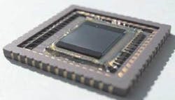
Key components networks
To satisfy growing bandwidth demands for computer and information technology, two basic strategies to increase the capacity of a system are applied: use a faster, larger, or more powerful system; or distribute the task to several identical subsystems working in parallel.
The semiconductor industry has shown much success in exceeding all speed and capacity limits of single-processor systems. Nowadays, multicore central processing units and massive parallel processing seem to be the better choices to increase computing power. In photonics, the motivation to use parallel optical channels is somewhat different. Photons do not have as strong an interaction with their environment as electrons do. Using wavelength-division multiplexing (WDM), an optical fiber can be baseband-modulated at about 10 terabits per second before transmission losses of the optical fiber would limit transmission.
In photonics, the desire to use many channels in parallel is driven by the difficulty of multiplexing and demultiplexing; switching and routing is more difficult than transmitting data over a long distance. For parallel optical interconnections, the use of suitable array optics is essential for collimation of laser-diode arrays, for focusing many optical channels onto digital-light-processing mirror arrays, and for fiber coupling—even when the coupling joint requires rotation (see Fig. 3). Semiconductor manufacturing technologies like resist coating, photolithography, and reactive-ion etching are used for manufacturing of high-quality microlens arrays. With lateral precision in the range of 50 nm, the excellent lens-profile accuracy and array uniformity allow accurate alignment of such microlens arrays to subsequent optics or optoelectronics structures on the full wafer scale.
Microlens-array beam homogenizers
Beam homogenizers made from microlens arrays are used to obtain a uniform, so-called “flattop” illumination profile for collimated light beams from a laser or light-emitting diode. These homogenizers are based on the well-known principle of fly’s-eye condensers, a combination of microlens arrays and a large condenser lens. The most popular version is the “imaging homogenizer” in which two identical microlens arrays are located at a focal length’s distance from each other.3 The first microlens array divides the incident beam into multiple subaperture beamlets. Every subaperture contains a different part of the incoming intensity profile. The second microlens array, in combination with a spherical lens, acts as an array of objective lenses that superimposes the images of each of the subaperture beamlets in the first array onto the homogenization plane.
The size of the flattop depends on the pitch of the microlens arrays, the focal lengths of the microlens arrays, and the size of the condenser lens. Typical dimensions for the resulting flattop range from only 50 µm up to 0.5 m on the diagonal. The intensity distribution of a flattop profile obtained by using square aperture microlens arrays manufactured in wafer-based technology in fused silica can be extremely uniform. Square microlens arrays provide a fill factor better than 98%. For high-power lasers, care must be taken not to damage the second array by focusing the beamlets into the lens material.
Microlens-array beam homogenizers decouple the output illumination field from the properties of the incoming light beam. This is very important for excimer or any high-power lasers with unstable mode profiles. Typical homogenizer applications include laser ablation, mask or reticle illumination, metrology, and efficient coupling in all modes of multimode fiber.
Outlook
A fascinating example of array optics is the Very Large Telescope Array (VLTA) on Paranal Mountain in Chile. The telescope comprises four 8.2 m reflecting telescopes and several moving 1.8 m auxiliary telescopes, the light beams of which can be combined in the telescope’s interferometer. In interferometric mode, when all telescopes work together, the VLTA produces sharper images than any other telescope on this planet. Again, microlens arrays are used for tuning and testing of VLTA components.
To implement array optics, optical designers must understand how diffraction effects limit the space-bandwidth product of small objectives, how interference effects at periodic arrays will influence the far-field pattern, and have to find a reliable supplier for prototyping and serial production of suitable array optics.
REFERENCES
1. D. Gabor, “Improvements in or relating to optical systems composed of lenticules,” Patent UK 541 753 (December 1940).
2. J. Duparré and R. Völkel, Proc. SPIE 6196 (May 2006).
3. F.M. Dickey, S.C. Hoswade, and D.L. Shealy, “Laser Beam Shaping Applications,” Taylor and Francis, ISBN 0-8247-5941.
REINHARD VÖLKEL is CEO and KENNETH J. WEIBLE is COO at SUSS MicroOptics, Jaquet-Droz 7, CH-2000 Neuchâtel, Switzerland; e-mail: [email protected]; www.suss-microoptics.com.