Photonic Frontiers: Silicon photonics - Development of silicon photonics focuses on high-speed optical interconnects
The big push in silicon photonics is beginning to yield results. The goal is to break the electronic data-transmission bottleneck for moving signals between processing cores on a single integrated-circuit chip, between chips, or between backplanes. It has become a high-priority target for key players in high-performance silicon ICs, notably chip-maker Intel (Santa Clara, CA) and the Defense Advanced Research Projects Agency (DARPA). Their investment is beginning to pay off.
The state of the integration art has progressed to the point where silicon chips can manipulate light from external sources. Luxtera (Carlsbad, CA) has integrated a pair of 10 Gbit/s silicon transceivers. Each transmission channel modulates the output of a continuous-wave external indium gallium arsenide phosphide (InGaAsP) diode laser with the input electronic data stream. A holographic lens integrated in the chip directs the input laser light into a waveguide that delivers it to a silicon modulator. Received signals are collected by another integrated holographic lens, which directs them through a waveguide into a high-speed p-i-n detector flip chip mounted on the silicon.1
The ultimate “holy grail” is an integrated optoelectronic chip that can be made from silicon with standard semiconductor fabrication technology, process signals electronically, and generate its own optical signal with no external light source. That ultimate goal remains maddeningly elusive more than 15 years after the first reports of light emission from porous silicon. Yet developers from the University of California at Santa Barbara (UCSB) and Intel have now demonstrated hybrid lasers that are electrically pumped and look very promising, although they are not entirely silicon. Other components are also coming along, including high-speed silicon modulators and optical data buffers.
Hybrid evanescent laser
Intel attracted considerable attention when it reported laser action in a silicon waveguide, but because its approach was based on stimulated Raman emission, it inherently required optical pumping (see www.laserfocusworld.com/articles/248133). In the fall of 2005, John Bowers and his group at UCSB described a quite different type of optically pumped silicon-waveguide laser, which they called a “hybrid silicon evanescent laser.”2
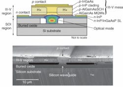
The crucial difference, easy to miss at the time, was that the hybrid design did not require optical pumping; it was just an experimental convenience. The Santa Barbara group fabricated a stack of III-V layers, grading from indium phosphide (InP) to an aluminum gallium indium arsenide (AlGaInAs) active layer containing five quantum wells, with an additional InP spacer and a stack of InP/InGaAsP strained layers. The group then mounted it on a 0.78 µm silicon rib waveguide etched from a silicon-on-silica substrate, using oxygen plasma-assisted wafer bonding. Dicing and polishing the structure left a 600-µm-long waveguide covered by the III-V stack.
Optically pumping with a pulsed 980 nm diode laser produced stimulated emission at 1538 nm, which coupled evanescently into the waveguide, causing laser oscillation in waveguide cavity modes-indicating the III-V region alone did not support laser oscillation. The UCSB group measured a 30 mW threshold, 3.2% slope efficiency, and output pulses to 1.4 mW.
The next crucial step was to replace the optically pumped III-V structure with one that could be excited electrically. Achieving that took ten months and some help from Intel.
The III-V structure for electrical pumping included n- and p-doped layers covering the whole area above and below the quantum-well active layer. It was bonded to a silicon-on-insulator substrate containing many parallel silicon rib waveguides, with the intervening spaces etched down to the oxide layer.3 After the III-V structure was bonded to the silicon, electrodes were fabricated to direct current through the active layer (see Fig. 1).
Experiments demonstrated continuous-wave laser action, with threshold current for laser emission from a single waveguide facet measured at 65 mA, and maximum output of 1.8 mW at 15°C. Output was near 1577 nm. The whole hybrid chip included 36 waveguides, 32 of which worked as lasers, although that many probes could not be hooked up simultaneously. The silicon waveguide has lower cavity losses, so it collects 90% or more of the light and controls laser emission; only a few percent of the light was in the III-V layer.
“The performance of this laser is pretty good for the first shot,” says Mario Paniccia, head of Intel’s silicon-photonics lab. He says the group has gotten better ones since submitting the paper. But what really excites him is the prospect for mass production. “It’s not about building one laser; it’s about how do we build hundreds.” A single operation can bond a broad-area III-V structure to a silicon substrate with 100 parallel waveguide stripes, forming 100 self-aligned lasers after final processing adds electronic contacts and carrier confinement.
Silicon modulators
Silicon modulators with data rates of 40 Gbit/s or more for high-speed optical interconnects are another challenge. Commercial lithium niobate electro-optic modulators operate at 40 Gbit/s, but they are costly discrete components. Silicon doesn’t exhibit the required nonlinear effects strongly enough for practical applications, although last September a group from the Department of Communications, Optics & Materials at the Technical University of Denmark (Lyngby, Denmark) reported silicon does exhibit the linear electro-optic (Pockels) effect.4
The best high-speed silicon modulators are based on a different effect, the modulation of refractive index caused by variations in current flow, called the free-carrier plasma dispersion effect. When this index modulation is applied to one arm of a Mach-Zehnder interferometer, the resulting phase delays modulate the output intensity. Luxtera’s integrated 10 Gbit/s modulator used this approach, with current flow modulated by incorporating a reverse-biased diode within the waveguide
Early this year, Intel reached a 3 dB bandwidth of 20 GHz, adequate to carry 30 Gbit/s. They applied a traveling-wave electrical input across one of a pair of parallel silicon rib waveguides in a Mach-Zehnder with reverse-biased p-n junctions running along their lengths (see Fig. 2).5 The waveguide cross section is very small, only 0.6 µm wide and 0.5 µm high, making it single-mode at 1.55 µm. The device was a compact 3 mm long.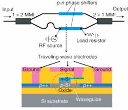
The developers say further improvements should be possible by optimizing the dopant profile and placement of the p-n junction in the waveguide. Drive voltage can be reduced by applying phase-shifted signals to both arms. They hope that other changes such as lowering the radio-frequency attenuation should help them approach the potential intrinsic bandwidth of 50 GHz.
Optical silicon photonics
Light sources and modulators alone won’t be enough to make high-speed optical interconnects. Packet switching requires buffers to store data while processors interpret address data, and simple optical-delay lines would be too cumbersome. Yurii Vlasov of the IBM Watson Research Center (Yorktown Heights, NY) and colleagues have made compact optical buffers by fabricating optically coupled silicon nanorings on a silica substrate. Light at 1550 nm makes about 70 circuits of each loop before moving on to the next, so an array of loops covering only 0.03 mm2 on the chip could hold 10 bits in a 20 Gbit/s data stream.6 A next step is to try to lower the losses.
Nor are optical interconnects the only application for silicon photonics. A small company called Enablence Technologies (Kanata, Ontario) has developed a compact 15 × 2 mm silicon photonic-waveguide triplexer for fiber-to-the-home connections that separates the upstream 1300 nm band from the downstream 1480 and 1550 nm bands.7 The Institute for Microstructural Sciences of the National Research Council of Canada (Ottawa, Ontario) has found that the strong, highly localized electric fields found in Mach-Zehnder and ring silicon rib waveguides makes possible highly sensitive evanescent-field biosensors.8
Outlook
The biggest stakes are in optical interconnects. Intel is looking toward chips with hundreds of cores in the next decade, according to Paniccia. “You’re going to need terabits of information moving in and out of processors,” he says. He thinks that target might be met by 25 parallel lasers, transmitting at different wavelengths, each modulated at 40 Gbit/s, and all mounted on a fingernail-size chip to produce a terabit of output (see Fig. 3). Plenty of work remains in improving, integrating, and producing devices. But Paniccia is optimistic that we’ll see some commercial silicon photonics-starting with discrete components and low levels of integration-by the end of the decade.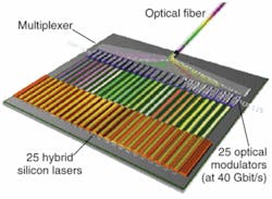
Developing technology for links inside data centers differs in crucial ways from developing long-haul telecommunications networks. One is that the much shorter distances eliminate a host of technical issues. “I can trade off a couple decibels of power for lower-cost packaging,” says Paniccia. Silicon photonics doesn’t need to match the performance of III-V transmitters. He says he would be happy with “90% of the performance for an order of magnitude in cost savings-that’s what you need to enable the high-volume marketplace.” Another is that these days the heaviest data transmission is short-distance traffic among chips and backplanes.
REFERENCES
1. B. Analui, IEEE J. Solid-state Circuits 41, 2945 (December 2006).
2. H. Park et al., Optics Express 13, 9460 (Nov. 14, 2005).
3. A.W. Fang, Optics Express 14, 9203 (Oct. 2, 2006).
4. J. Fage-Pedersen, L.H. Frandsen, A.V. Lavrinenko, and P. I. Borel, paper WC3 (invited), Proc. Third Int’l. Group IV Photonic Conference, CD-ROM (IEEE, Piscataway NJ, 2006).
5. A. Liu et al., Optics Express 15, (Jan. 22, 2007)
6. F. Xia, et al., Nature Photonics 1, 65 (January 2007).
7. S. Bidnyk, et al., paper P28, Proc. Third Int’l. Group IV Photonic Conference, CD-ROM (IEEE, Piscataway NJ, 2006)
8. A. Densmore et al., paper WA2, Proc. Third International Group IV Photonic Conference, CD-ROM (IEEE, Piscataway NJ, 2006).
About the Author

Jeff Hecht
Contributing Editor
Jeff Hecht is a regular contributing editor to Laser Focus World and has been covering the laser industry for 35 years. A prolific book author, Jeff's published works include “Understanding Fiber Optics,” “Understanding Lasers,” “The Laser Guidebook,” and “Beam Weapons: The Next Arms Race.” He also has written books on the histories of lasers and fiber optics, including “City of Light: The Story of Fiber Optics,” and “Beam: The Race to Make the Laser.” Find out more at jeffhecht.com.