SILICON PHOTONICS: Silicon/organic hybrid laser produces red light
A team at the Organic Semiconductor Centre of the University of St. Andrews (St. Andrews, Scotland) has demonstrated a hybrid silicon (Si)/polymer surface-emitting red laser. The new laser, in which the role of the polymer is to add light emission to Si, operates at room temperature, is tunable, and could become a low-cost light source for chip-to-chip communication.
Because of the material’s wide use and mass-fabrication possibilities, Si-based photonic devices are attractive as the basis for cost-effective integrated components for optical communications and interconnects. Unfortunately, Si itself is a very inefficient light emitter. The St. Andrews researchers have overcome this limitation by combining Si resonators with light-emitting organic semiconductors, which can be added by simple solution deposition.
The team faced two major challenges in designing a successful hybrid device. First, Si strongly attenuates light in the wavelength range of the polymer photoluminescence. And second, the high refractive index of Si complicates the confinement of any laser emission within a polymer waveguide.
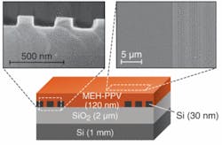
To overcome these issues, the team relied on a distributed-Bragg-reflector (DBR) resonator design fabricated on a silicon-on-insulator substrate (see figure). Microstructuring was achieved with a combination of reactive-ion etching and electron-beam lithography. Two DBR mirrors were created 50 µm apart; the Si epilayer between the mirrors was removed, exposing the buried silicon oxide (SiO2) layer. A thin film of the organic amplifying medium, MEH-PPV, was used to cover the whole structure. The boundary conditions at the air-polymer and polymer-SiO2 interfaces ensured that a polymer waveguide was formed between the two Si mirrors. The effective result was a long “defect” in the Si DBR photonic lattice, which minimized the interaction of the laser light with the Si regions, thus minimizing absorption of laser light.
The device was optically pumped; 1.2 ns pulses from a frequency-doubled microchip emitting at 532 nm were focused into the area between the mirrors. The resulting surface emission was collected by a fiber-coupled spectrometer. To avoid photo-oxidation, the polymer films were held in a vacuum of around 10-4 mbar during testing.
“The lasers we generated were tunable from 608 to 628 nm, and were pulsed at 5 kHz with pulse energies in the picojoule range,” says Graham Turnbull, one of the researchers. “Lengthening the cavity allows us to produce more than one longitudinal mode to operate at the same time, which may prove useful. The light emission is in the visible region of the spectrum, so it is readily detected by silicon photodiodes, making it suitable for low-cost chip-to-chip communications.”
The team has plenty of ideas for future developments. “This work has demonstrated the principle of the hybrid laser,” says Turnbull. “The next challenge is moving to electrical excitation. We can envisage using the underlying silicon chip to apply a field or inject charge to modulate the light emission. In the longer term, electrically pumped lasing using p-doped silicon as a hole-injection layer is also a possibility.”
