DETECTORS: Micro cameras ignore the diffraction limit
CHRISTOPHER M. AUBUCHON
The technology design and integration necessary to miniaturize a camera module for use in portable electronics involve a complex interdependence of six technical, financial, and qualitative factors: module size, cost, image quality, relative aperture size, special features, and the silicon image sensor.
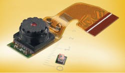
The overall module size is constantly shrinking and z-height reduction is critical for use in thin-form-factor products (see Fig. 1). Cost is widely recognized as the largest driver of the overall module and thereby restricts the complexity of design. The output image quality of a camera is a subjective measure that is pushed to be the best possible, within cost constraints. The relative aperture size (or f-number) of a camera module affects its light-gathering ability and thereby drives low-light performance, an image-quality criterion gaining greater attention as users increasingly take candid photos in poor lighting situations. Special features like autofocus, zoom, and anti-shake can be added to the camera to increase functionality and serviceable market size.
The image sensor, or “silicon”-including image-sensor-processor (ISP) functions-is the most critical component that affects cost, functionality, and quality of the end product. In state-of-the-art camera designs, the silicon works alongside the optics, affording optical-module designers the ability to reduce their dependence on the modulation-transfer function (MTF; see www.laserfocusworld.com/articles/250403) and ignore the diffraction limit. Further, camera-module manufacturers are capitalizing on the economies of scale commonly associated with semiconductor manufacturing, using etching, stacking, and bonding techniques on glass wafers for mass manufacturing of lens systems at micron tolerances.
Image-sensor characteristics
Over the past decade, pixel sizes in standard complementary-metal-oxide-semiconductor (CMOS) sensors have followed a shrinking trend from 5.6 µm (on a side) to the current standard of 2.2 µm.1 Array sizes have not miniaturized as quickly, however, because of the desire for higher-resolution photos.
With the 1/4 in. image sensor beginning to define a de facto standard for camera modules, a 2.2 µm pixel size results in 2-megapixel (MP) product lines. Image-sensor companies approximate the product roadmap for the 1/4 in. imager as decreasing from 1.75 to 1.4 µm and down to 1.2 µm pixels, the latter resulting in a 6 MP image sensor.2 This roadmap creates a problem for camera designers because of the decreased pixel size and lower signal level at a given illumination.3, 4 However, each generation of silicon is designed with inherent functions and compensation for the limitations implicit to the pixel size and architecture (see www.laserfocusworld.com/articles/274731).
Optics and image-processing capabilities
Traditionally, the optical design was an optimized diffraction-limited system, leading to a through-focus MTF that showed a peak at the focus. As an object moved away from the focal point, image aberration would increase at the image plane. More than 30 years ago mathematicians recognized that image processing could recover some elements of the aberration, but image sensing and computational capabilities then were still in their infancy.5 Today, the system is designed with paired components: physical lenses optimized to perform specific transfer functions and algorithms-either utilizing transistor logic gates in the ISP or cycles in the application processor-optimized to perform deconvolution algorithms for which the sensor architecture is well suited.
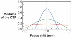
The through-focus MTF magnitude gives a general figure of merit to an imaging-system design, but optimal image quality post-processing is the target (see Fig. 2). Compared to a diffraction-limited design, an alternative design can have a lower MTF at the focus, but objects at half the focal distance are less blurry. Still other designs can have a nearly uniform MTF over the widest depth of field. The images from the latter two designs will not appear as crisp at the image plane, but after careful processing, the images can become visually comparable to the diffraction-limited design, and even superior at varying points of field depth.
As a result, intelligent codesign of optics and algorithms becomes the foundation in the unification of the six factors that influence camera miniaturization.6 Embedded in this foundation are additional features that can be added to the end product. For instance, by utilizing advanced optics and smart algorithms, it is possible to implement many useful features such as digital autofocus, zoom (optical and/or digital), antishake, image stitching, image recognition, tracking, and countless others-without any moving parts.
Light limitations
A common complaint from users of miniature cameras is poor low-light performance-a burden shared by the optical and silicon design of the camera. Optics can hinder the light-level performance by reducing the resolving power of the lens system or simply by having too small of an aperture to allow adequate illumination of the sensor elements. The silicon is burdened by the trend toward smaller-area pixels leading to significantly lower lumens per pixel. Following the declining pixel-size trend over the past decade, pixel area has shrunk by a factor of almost seven and by 2010 it is forecast to shrink by three times more.
To compensate for the reduced lumens/pixel in the sensor, the optical-system design must try to capture more photons from a given scene. Increasing the aperture allows a greater amount of light to enter the pupil and fall on the image plane. This is one way design engineers can improve low-light performance as pixel sizes decrease, but at a tradeoff to other metrics such as depth of field, spatial resolution, and resulting image quality.
Improved image quality
The term “megapixels” still has marketing pull for consumers and is a dominant factor in driving product roadmaps. However, the megapixel appeal dwindles as consumers begin to scrutinize the sharpness, clarity, and color of the output image.
To help create a consumer-friendly image-quality metric, the Camera Phone Image Quality (CPIQ) Initiative group-a formal Initiative within the not-for-profit International Imaging Industry Association (I3A; www.i3a.org)-was formed with a goal to define an objective metric or standard. Independent of CPIQ pursuits, OEMs are trying to stay ahead of the consumer with their metric of choice for imaging applications being the signal-to-noise ratio (SNR) of the output image. Increasing the SNR of next-generation designs is handled predominantly in the silicon but can be helped by improving the quality of the optics, design, materials, or assembly process. Using a glass lens instead of a plastic element, for example, can noticeably increase the image quality. Subtle changes that decrease stray light, increase MTF, or reduce poor-tolerance manufacturing can make a remarkable difference in the optical efficiency of the system, while innovative algorithms can further improve the output image quality.
Cost is king
Conventional camera-module assembly involves manual labor, barrel assemblies, and flex leads to allow reflow. In conventional systems, a miniature chip-on-board assembly incorporates an image sensor, barrel assembly, and flex-circuitry. Various optical elements are inserted, adjusted, and optimized within the barrel, often by hand. A typical module has a half dozen parts that are all integrated at varying levels of the supply chain. To reduce costs and increase profitability, the value chain is contracting toward more vertical integration, so the lens and module assemblers are becoming one-stop shops and the innovative algorithms of the ISP are being implemented at the sensor level. The consolidation of the entire supply chain to wafer-level manufacturing can reduce manufacturing costs by an estimated 30%.
Reducing camera size
Minimizing overall camera-module volume is an important aspect of the design process. The physical specification can drive the total track length of the through-lens optical path, which affects the lens design of the entire system. Image-sensor size is the first specification that determines the design parameters that influence the final module, and the optical design relies on the type/composition of materials that will be involved in the lens. Using glass provides better optical quality and more uniformity than plastic, but at a different cost, index of refraction, weight, and manufacturing-tolerance demand. Higher-index-material lenses allow for tighter focusing in smaller path lengths, but this comes at a cost premium.
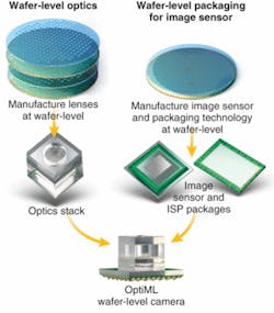
Lenses are manufactured to their specifications by using various semiconductor techniques of etching, stamping, embossing, and/or deposition for each individual glass wafer surface. Once the lens wafers are completed they can be aligned, united, and diced prior to placing the individual lens stacks on their respective image sensor. This massively parallelized process leads to large numbers of optics made with semiconductor precision and scalability. For example, a single 6 in. wafer stack can yield more than 6000 lens modules, further driving down manufacturing costs. The lens stack is then pick-and-place affixed to packaged image sensors, eliminating the need for manual adjustment to the lenses in the barrel assembly. This wafer-level optical technique (called OptiML) results in very small camera modules (see Fig. 3).
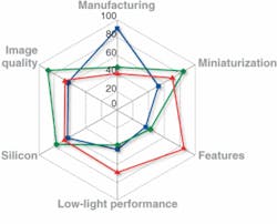
Not only do camera-module designers recognize the interplay of the six variables presented, but they also have access to advanced optics software to optimize various design parameters. The design process no longer entails a diffraction-limited imaging system wrapped into a complete package. Today, the best designs are found by balancing the many tradeoffs of the parameters that contribute to the final module design (see Fig. 4). While MTF is a valid technical figure of merit, the image quality produced by the system is more relevant. The optics and algorithms work in concert to provide the best post-processed SNR, contrast ratio, spatial resolution, and color fidelity, which comprise the best measures of quality for a miniaturized camera module.
null
REFERENCES
1. Direct market data provided by Techno Systems Research Co. (TSR)
2. P. Rosdahl and H. Gadjali, Image Sensors 2007, San Diego, California (June 25, 2007).
3. J. Farrell, F. Xiao, and S. Kavusi, Proc. SPIE6069, 211 (2006).
4. P.B. Catrysse and B.A. Wandell, J. Optical Society of America A19(8) 1610 (2002).
5. J.W. Goodman, Introduction to Fourier optics, 2nd ed., McGraw-Hill, New York, NY (1996).
6. P. Maeda, P.B. Catrysse, and B.A. Wandell, Proc. SPIE5678, 48 (2005).
Tell us what you think about this article. Send an e-mail to [email protected].
CHRISTOPHER M. AUBUCHON is director of technology strategy at Tessera, 3099 Orchard Dr., San Jose, CA 95134; e-mail: [email protected]; www.tessera.com.


