PLASTIC OPTICS: Process integrates active and passive polymers
Successful lab-on-a-chip sensors that incorporate solid-state polymer lasers with large free-spectral-range values require that the associated polymer gratings in the laser cavity have subwavelength features (on the order of 100 nm). Although interference lithography and thermal nanoimprint lithography (TNIL) can be used, pattern flexibility is limited with interference techniques and TNIL has difficulty defining larger structures and leaves a residual polymer layer that requires additional steps to remove. To overcome these obstacles, researchers at the Technical University of Denmark (DTU; Lyngby, Denmark) have demonstrated a low-cost wafer-scale process that integrates active-polymer distributed-feedback (DFB) lasers and passive-polymer waveguides with nanometer-to-millimeter feature sizes and no residue.1
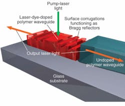
The polymer DFB lasers are fabricated using combined nanoimprint and photolithography (CNP). In the CNP process, nanometer-size features are imprinted in a photodefinable polymer that is then selectively hardened on the nanometer-to-millimeter scale by ultraviolet (UV) exposure through a shadow mask. Specifically, the lasers were Rhodamine 6G-dye-doped SU-8 polymer slab waveguides (cladded by the silicon dioxide substrate and air) with first-order Bragg feedback provided by approximately 2500 surface corrugations on each side of the central cavity structure (see figure). These corrugations had periods ranging from 187 to 202 nm, with corrugation depths of 10 to 60 nm. The fabricated lasers had a footprint of 1 mm by 250 µm and were each 245 nm high (thin enough to support only a single TE-TM mode).
Depending on the grating period (187, 192, 197, or 202 nm), the laser’s emission wavelength could be varied (557, 572, 587, or 602 nm, respectively) when pumped from above the chip with 5 ns pulses from a 532 nm frequency-doubled Nd:YAG laser.
After laser fabrication by CNP, SU-8 polymer waveguides were added to the chip using standard UV lithography. The 4.2-µm-thick waveguides tapered in width from 250 to 100 µm and were curved (radius of curvature 4 mm) to guide the laser output to the edge of the chip.
To test the integrated devices, the output from the Nd:YAG-pumped DFB laser and SU-8 waveguide was collected by a multimode fiber and fed to a spectrometer. The laser was tested at room temperature and at various other temperatures by placing the laser on a Peltier element. All lasers emitted TE-polarized light at wavelengths based on their respective internal grating periods. These wavelengths could each be tuned by a few nanometers through external temperature control.
Although the laser dye bleaches when pumped at 10 Hz with 20 µJ/mm2 pulses (causing the output to halve in a few hours), this lifetime is still acceptable for single-use lab-on-a-chip systems. “The CNP fabrication method is very flexible, and not limited to making devices on flat glass substrates,” says researcher Mads Brøkner Christiansen, who is now working on applying the technology for optical sensing. “In the future, we could imagine using the fabrication process for adding optical functionality at different points in larger prefabricated systems; for instance, an optical detection system could be added to a container for blood samples.”
This work was performed within the European Union FP6 Integrated Project “Emerging Nanopatterning Techniques” (www.napaip.org). “The laser performance—lasing wavelength and threshold—depends critically on the nanoscale feature sizes, and the high reproducibility we have obtained documents nanoscale feature-replication fidelity and homogeneity on the wafer scale,” says professor Anders Kristensen.
REFERENCE
1. M.B. Christiansen et al., Optics Express 15(7) 3931 (April 2, 2007).
About the Author

Gail Overton
Senior Editor (2004-2020)
Gail has more than 30 years of engineering, marketing, product management, and editorial experience in the photonics and optical communications industry. Before joining the staff at Laser Focus World in 2004, she held many product management and product marketing roles in the fiber-optics industry, most notably at Hughes (El Segundo, CA), GTE Labs (Waltham, MA), Corning (Corning, NY), Photon Kinetics (Beaverton, OR), and Newport Corporation (Irvine, CA). During her marketing career, Gail published articles in WDM Solutions and Sensors magazine and traveled internationally to conduct product and sales training. Gail received her BS degree in physics, with an emphasis in optics, from San Diego State University in San Diego, CA in May 1986.