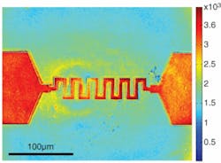
Thermoreflectance imager sees microscopic IC features through silicon
Visualizing hot areas in integrated circuits (ICs) at microscopic scales can be key to identifying potential underperformance or failure. Thermoreflectance measurement, in which local reflectivity changes induced by heating are monitored, is one approach. But because many problems occur in deeply buried regions (especially in flip-chip configurations), simple surface imaging will not work. And seeing things to submicron scales is difficult because of the necessity of using IR light at 1.1 µm or longer wavelengths.
Researchers at ESPCI (Paris, France) have developed a thermoreflectance imager for ICs that can include a very high-numerical-aperture silicon immersion lens (SIL) to boost resolution, and incoherent (1.1-1.7 µm) illumination to eliminate interference from multiple reflections. The numerical aperture of 2.36 results in a resolution of 440 nm. A SIL with a radius of 3.5 mm paired with an indium gallium arsenide image sensor allows imaging through a 500-µm-thick silicon substrate. Here, a gold resistor dissipating 609 mW is imaged at a 1.7 µm resolution (without the SIL); the temperature increase in the nearby silicon is 27 K. Contact Gilles Tessier at [email protected].

