Compliant MEMS provide stiff competition
By Michael Little
In the last few years, optical networking has spawned new applications for the technology known as MEMS (microelectromechanical systems). With tiny mechanical devices, such as sensors and mirrors, embedded in semiconductor chips, MEMS technology allows electronic systems to sense and control light, making it ideal for use in optical networking equipment. Additionally, MEMS devices have fewer discrete components than devices of rival technologies, so they provide better reliability at lower cost, and a more compact package design permits superior integration.
Previously, MEMS was deployed in the laboratory when small robotics were needed to develop products and processes. It has also been incorporated in products such as medical display devices and automobile airbag accelerometers, using electrostatic or magnetic forces to bend or deflect one of the MEMS layers to produce a desired mechanical motion.
Recently, several MEMS products have been introduced into the telecommunications industry, including optical switches and crossconnects. These devices are made of traditional silicon-based MEMS materialsvery rigid and noncompliant, with a Young's modulus of about 160 gigaPascals (GPa). In addition to their stiffness, silicon-based materials have very low yield points, typically less than 1%, which means they cannot be stretched, bent, or twisted very much before they break.
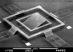
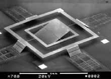
Accordingly, the spring hinges that form the gimbal supports for an optical crossbar switch, for example, must be thin, delicate structuresno more than a few micrometers in depth in the lateral dimension (see Fig. 1). As a result, very precise lithography is needed to define the width of the silicon supporting the micromirrors. This limited range of mechanical properties and thickness severely narrows the design space for silicon-based MEMS devices. Moreover, the extreme rigidity of silicon MEMS requires higher voltage to provide the force for mechanical deflection.
Compliant MEMS technology
Just as the demands of optical networking called for the application of MEMS technology, the limitations of silicon-based MEMS have brought about a dramatic new approach, manifested in a new class of MEMS devices that uses, for the first time, highly compliant polymeric materials as a principal design element.
The compliant MEMS (CMEMS) platform differs from conventional MEMS by adding a set of softer, more malleable materials to the conventional list of rigid silicon-based materials that can be deposited, patterned, and etched. Robust and simple in its design, CMEMS technology uses a soft, rubber-like material called an elastomer that can be stretched by as much as 300%, (compared to less than 1% for silicon). The material itself is not new; it has been around for about 50 years. NASA is currently using it on various space shuttle components, so it has withstood some very adverse environments.
To date, elastomers have been used in MEMS devices primarily for microfluidics and microvalve applications. For these applications, silicone-based elastomers are used for their ease of molding and sealing properties. Unlike other elastomers, silicones have a SiOSi backbone, instead of a CC backbone, which gives them excellent mechanical, chemical, and thermal stability. Many silicones can withstand up to 200% strain-to-failure.
From a design perspective, elastomers are very attractive mechanical members for electrostatic actuators. Compared to other actuation mechanisms, electrostatic actuators are relatively weak, requiring correspondingly weak mechanical members. In traditional MEMS materials, such as silicon and silicon nitride, this translates into very thin structures.
Instead of a Young's modulus of 160 GPa, the rigidity of the elastomer can be as low as 200 kPa, or six orders of magnitude less stiff than silicon MEMS, and it can be tailored over a range of three orders of magnitude. Accordingly, elastomers can be used in much thicker cross sections. In addition, CMEMS devices made with elastomers require much lower voltages to achieve a given mechanical deflection, and their mechanical range of motion is much larger than with silicon MEMS for equivalent voltages. This pronounced modulus difference also allows for the design of shear mode as well as bending mode devices. Shear mode devices have two principal advantages in that they inherently resist off-axis movement and are less sensitive to variations in dimensions during manufacture.
In addition, the elastomer can be deposited in layer thicknesses of 1 μm to 1 mm, a very wide range of flexibility that significantly expands the design space for MEMS devices beyond what is possible with traditional silicon-based materials. Because the elastomer is more compliant than silicon, its geometries can be defined less precisely in the lithography process.
Another advantage of CMEMS is in the deposition method itself. Silicon MEMS uses chemical-vapor deposition techniques, in which "sacrificial" layers are deposited on top of a silicon wafer to create a structure. This requires a large, complex, and expensive machine. Conversely, CMEMS technology uses spin-on deposition to pattern a structure. With this technique, a silicon wafer is placed on a chuck that spins at a high speed; elastomer is then deposited, leveling out to form a thin, smooth layer on top of the wafer. The same spin-on equipment is smaller, simpler, and considerably less costly than the chemical-vapor deposition machine, and the process is also faster.
Applications
Currently being readied for introduction is a tunable optical filter, or interferometer, that incorporates the new CMEMS technology (see Laser Focus World, September 2001, p. 41). Tunable filters, which transmit light of a predetermined wavelength and reflect the nontransmitted light back toward the source, are used in a variety of optical networking equipment, including optical performance monitors. As network providers adopt higher data rates and denser channel spacinghundreds of channels in a single fiberperformance monitoring becomes increasingly critical because individual optical signals have a greater chance of being lost or degraded. This could cost a service provider as much as $10,000 per minute per channel.
Although interferometers can be achieved using several different methods, the most commonly used in optical networking applications is the Fabry-Perot-based tunable filter. Recent Fabry-Perot filters have used silicon-based MEMS technology to control the separation between the plates, but maintaining the necessary tight tolerance on the plates' parallel orientation is complex and expensive. Besides requiring high voltages, these filters also have a relatively narrow operating-temperature range. This makes manufacturing and assembly difficult and labor-intensive, which adds cost to the devices and makes them less reliable.
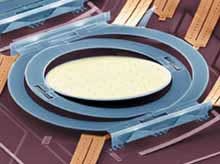
The new CMEMS-based tunable filter is a Fabry-Perot interferometer that includes an elastomer donut bridging a silicon island and a frame. Based on a simple mechanics analysis of the device, it has an effective spring constant given by
null
where k is the spring constant, h is the wafer/elastomer thickness, r is the radius of the island, d is the width of the elastomer donut, G is the shear modulus, E is Young's modulus, and υ is Poisson's ratio. Silicone-based elastomers have a Poisson's ratio of 0.5, which makes them incompressible.
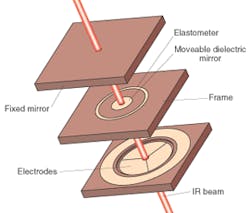
The new tunable filter is designed as a three-layer sandwich of micromachined silicon wafers (see Fig. 2). The first layer is a silicon substrate with a high-reflectivity dielectric mirror on its interior surface and a high-efficiency antireflection coating on its outside surface. The second layer contains the high-reflectivity movable mirror that is the tuning element of the Fabry-Perot. It has a high-reflectivity dielectric mirror deposited on a silicon island that is suspended from a perimeter frame using a compliant elastomer layer. Three segmented electrodes on the backside of the elastomer layer match up with electrodes contained on the third and final layer. Voltages applied between the second and third layers control the gap between the first two layers, while the segmented electrodes enable precise adjustment of the Fabry-Perot cavity.
The CMEMS technology delivers high finesse of up to 2000 for superior channel selectivity, high filter contrast of 40 dB for precise measurements of optical power and signal-to-noise ratio, and insertion loss of less than 2.5 dB. These factors all combine to lower production costs and improve yields for CMEMS components, an especially important consideration in the telecommunications industry as it deploys denser and higher bandwidths to boost optical network capacities.
Although silicon-based MEMS interferometers can also deliver very high finesse and low insertion loss, attaining these specifications is much harderresulting in higher costs, lower yields, or the degradation of some other performance metric. There are times, however, when traditional silicon-based MEMS technology is preferable to its new silicone-based cousin. In automotive applications, for example, silicon has the advantage because there's not a lot of precision involved. Basically, the end product is a sensor or a transducer, without much need for specific performance. Compliant MEMS can certainly be used in such applications, but not to the advantage of its inherent strengths.
In the foreseeable future, then, CMEMS technology will provide the most value in the world of optical networking, with its urgent need for tunable components that enable new levels of functionality and performance. Compliant MEMS promises to enhance next-generation tunable lasers, multiplexing/demultiplexing filters, gain-flattening devices, dispersion-compensation devices, and other components that increase the agility of the optical network.
MICHAEL LITTLE is vice president, chief technical officer, and cofounder of Solus Micro Technologies Inc., 5706 Corsa Ave., Westlake Village, CA 91362; e-mail: [email protected].


