Diffractive MEMS technology offers a new platform for optical networks
By Asif Godil
Dynamic components are a new breed of device that complements traditional active components (lasers, detectors, modulators) and passive components (multiplexers, isolators, circulators, couplers). First-generation dynamic components have historically included motor-controllable variable optical attenuators (VOAs) and bulk mechanical switches. These early dynamic components did not meet the requirements for integration and compactness. Using microelectromechanical systems (MEMS), dynamic components now include optical crossconnects, switches, VOAs, gain equalizers, channel equalizers, tunable filters and lasers, dynamic dispersion control, and programmable optical add/drop multiplexers.
Mention MEMS and most people immediately think of micromirrors and shutters, particularly in fiberoptic applications. However, there is no single MEMS technology. Any device that utilizes micromechanical structures is a MEMS, and there are many variations with different operational characteristics and manufacturing processes for fabricating them. Some achieve greater performance and reliability with simpler, less costly manufacturing, while other MEMS types rate lower in these areas.
Mirrors, for example, require a highly specialized, nonstandard fabrication process that can dramatically raise the cost of production. The relatively large movement of mirrors makes them more susceptible to ambient acoustic noise and vibration. Another approach based on a moving shutter utilizing a thermal bimorph may consume more power.
A different approach, known as diffractive MEMS (D-MEMS), is better suited for these dynamic component applications. The D-MEMS platform uses the wave aspect of lightinterference and diffraction. The basic technology, originally referred to as deformable grating modulators, was developed at Stanford University in the early 1990s.1
The Stanford approach
The approach pioneered by the Stanford group involves an array of ribbons suspended one wavelength (l) above a silicon substrate (see Fig. 1). In this state, the D-MEMS device looks like a mirror. By applying a small voltage to the ribbons, the electrostatic force pulls them down, effectively turning on a phase grating. Light is diffracted out and the main beam is attenuated, hence the term diffractive MEMS.
This technology has many advantages over other types of MEMS. The simple, noncontact operation requires very small movements (<0.4 μm). Because the ribbon only has to deflect a few tenths of a micron, the structure can be made very stiff. This stiffness, together with low mass, results in a high resonant frequency and fast response times in the tens of microseconds.
The D-MEMS structure is inherently reliable and rugged. Devices have been actuated more than 50 billion times in the lab with no measurable change in performance and have been qualified according to Telcordia GR-1209 and GR-1221.2 Devices have been vibrated at up to 20-G acceleration and up to 2-kHz frequency while operating at 15-dB attenuation with little effect on the performance. In comparison to thermal or magnetic actuation-based MEMS, the capacitor-like D-MEMS consumes less energy and does not dissipate excess power.
Because of its planar nature, a D-MEMS device can be fabricated in a typical 1.0-μm CMOS foundry using standard fab processes. This common process is available from multiple sources, thereby ensuring a reliable supply as well as manufacturing flexibility. This is in contrast to mirror- or shutter-based, or other MEMS that require specialized fabrication facilities, equipment, and clean rooms.
The D-MEMS fabrication process begins with oxidized silicon wafers, upon which a sacrificial layer of polysilicon is deposited, patterned, and etched. To form the ribbon array, a silicon nitride layer is deposited, patterned, and etched. The mechanical layer consists of low-pressure chemical-vapor deposition (LPCVD)-deposited silicon nitride, one of the most rugged materials in the silicon industry with high yield strength of 20 Gpa. The polysilicon sacrificial layer is etched away, releasing the ribbon array. Finally, the ribbon array and the substrate are aluminum coated. This coating functions as a reflective surface for the light and as an electrical path for the control voltage. Conventional 1.0-μm lithographic processes are used throughout the process.
To create a device such as a compact variable optical attenuator, conventional fabrication processes are used. A VOA MEMS chip is mounted on a standard TO-39 header for low-cost manufacturing. A two-fiber capillary is aligned in front of a graded-index lens mounted on a Kovar cap. Automated alignment provides reliable, efficient, and rapid manufacturing. The Kovar cap is projection-welded to the header, providing a hermetic package for the MEMS chip. The resulting VOA measures 9 mm in diameter by 17 mm.
Limitations of the Stanford approach
Application of the Stanford approach to fiberoptic technology began in 1998, leading to the development of a high-performance fast VOA and a dynamic gain equalizer (DGE) for flattening erbium-doped fiber amplifiers (EDFAs). Early on, two major limitations of the Stanford approach were discovered: spectral dependence and polarization dependence.
As the attenuation is increased, it is not spectrally flat across a given wavelength band (see Fig. 2). Phasors E1 and E2 interfere or add to produce the resultant output field, Et. They are of equal amplitude and the phase, φ between them is adjusted using a control signal. When φ is small or zero, the light is mostly transmitted with very little attenuation. Rotating E2 by π cancels E1, such that Et = 0, giving maximum attenuation.
This is only true for the center wavelength, λc, however. For wavelengths either above or below λc, the phasor E2 rotates more or less than π, giving an effective error vector, ΔE2. This becomes the error on the output light; in other words, ΔEt = ΔE2, and the output light spills over on both sides of the center wavelength. Consider such a device at 15-dB attenuation across the 40-nm C-band. Calculations show a wavelength-dependent loss (WDL) of about 1.7 dB, which is highly undesirable for many system applications. The Stanford design is even worse from a WDL perspective. The conventional phasor picture applies here as well, except that φ starts out at 4π in the on state and goes to 3π in the maximum attenuation state. In this case, WDL at 15-dB attenuation across the C-band is 6.2 dB. This is indeed unacceptable for many applications.
An elegant solution
A simple and elegant solution uses an achromatic design, which leads to very low WDL (see figure, p. 181). Consider a device with ribbons of two different widths, w1 and w2, which are separated by a gap of g/2. Again, the entire surface is coated with a reflective layer of aluminum. One period of the device is then composed of w1, w2, and two g/2 gaps (2 x g/2 = g). The ribbons are nominally positioned a distance ts above the substrate. Let ts = 1.5λ, which corresponds to a round-trip phase of 6π. Assume w2 = w1 + g. The phasors corresponding to these regions are shown as E2, E1, and Eg. In the nominal state (φ = 0), E1 and E2 are at zero phase with Eg at 6π phase. The output field, Et, is at maximum at this point with zero attenuation.
Applying a voltage to the wider ribbon (w2) deflects it downward. This rotates phasor E2 by an amount φ until it reaches π when the deflection is λ/4. In this state, E2 cancels E1 + Eg, giving Et = 0 (maximum attenuation). But now, as the wavelength varies above or below λc, the error vector on E2 sticks out as ΔE2. However, now an error vector on Eg of ΔEg also sticks out in the opposite direction. Eg is at 6π phase while E2 is at π. Therefore, when Eg = E2/6, the two error vectors cancel each other; in other words, ΔEt = ΔEg + ΔE2 = 0. This leads to achromatic attenuation. At 15-dB attenuation, calculations predict a wavelength-dependent loss less than 0.1 dB. In practice, wavelength-dependent loss less than 0.4 dB is routinely obtained.
Because of the ribbon structure, the device is not symmetrical in the two orthogonal directions. This lack of symmetry leads to polarization-dependent loss, which gets worse with attenuation.
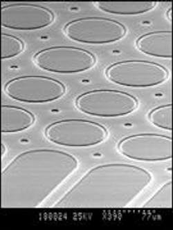
The solution was to create a grating structure that is perfectly symmetrical in the two directions. The polarization-independent device is effectively a two-dimensional phase grating. The achromatic aspect is also included in the design. The round discs are fixed islands of height ts, which form the E1 phasor in the achromatic design. The membrane around the islands has tethers going toward anchors that form the E2 phasor. The gap between the membrane and the island and the small release holes in the membrane comprise the Eg phasor. The incoming beam illuminates several unit cells in each direction. By applying a voltage to the membrane, achromatic attenuation is accomplished. This device forms the basis of the achromatic design VOA.
REFERENCES
1. O. Solgaard, F. S. A. Sandejas, and D. M. Bloom, Opt. Lett. 17, 9 (1992).
2. http://telecom-info.telcordia.com
ASIF GODIL is chairman and chief technology officer of Lightconnect, 35445 Dumbarton Ct., Newark, CA 94560; e-mail: [email protected].


