In optical lithography, photons of shorter and shorter wavelengths are being used to achieve ever-finer patterning of semiconductor integrated circuits, with wavelengths reaching to the extreme-ultraviolet and even x-ray spectral regions. Using atoms for lithography, however, should allow the fabrication of feature sizes even smaller, as the de Broglie wavelengths of atoms amount to only a few tens of picometers.
One fascinating aspect of lithography by atoms is the possibility of controlling the atomic trajectories by light, replacing mechanical patterning masks by flat, locally structured stationary light fields generated by the interference of laser beams. In such an inhomogeneous electromagnetic field, dipole forces act on an atom whenever the frequency of radiation is close to a resonance frequency of that atom.
Depending on the direction of detuning from resonance, dipole forces can be either attractive or repulsive. Detuning to a shorter wavelength, for example, bends an atomic trajectory to regions of lower field intensity so that atoms concentrate at the nodes of the field; consequently, the atoms form a similarly modulated flux density that can form a corresponding pattern on a nearby substrate. The approach was invented at AT&T Bell Laboratories (Murray Hill, NJ) in 1992 by use of a standing light-wave field, resulting in structures of parallel lines.1
3-D atom lithography
Interference-induced structured light fields cannot provide the abrupt bright-to-dark contrast of a mechanical mask; however, there are applications that do not require abrupt contrast—for example, in micro-optics where the index of refraction may vary continuously. Furthermore, because of focusing of the atoms by the light field, light-induced atom lithography with sharper edges can be realized. Now, a three-dimensional (3-D) atom lithographic technique has been developed by a research group at the University of Bonn (Bonn, Germany).2
In the technique, two-dimensional inhomogeneous light fields are successively created by one laser beam so that 3-D structures can be readily built up. A standing-wave light field serving as the mask is generated above the substrate by the interference of two Bragg-reflected beams from a volume hologram with the incoming coherent beam. The hologram is stored in a lithium niobate nonlinear crystal; many other holograms also can be stored there, readable by angular tuning.
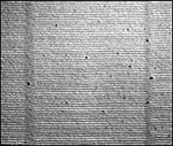
The researchers demonstrated the structuring of just one layer but emphasized the potential of the holographic method for multiple layers. Atom lihographic capability was demonstrated by focusing transversely laser-cooled cesium (Cs) atoms on a dual-layer system deposited on a silicon substrate and consisting of a gold layer covered by a thin layer of the organic compound nonanthiole. Cesium atoms were typically evaporated for 90 s at a flux density of 5 x 1012 cm-2s-1, resulting in an approximate monolayer with the flux transversely modulated according to the light mask. The Cs chemically modified the nonanthiole; the gold underneath could then be etched off so that the surface of the silicon appeared at the corresponding regions. A pattern obtained in this way consists of horizontal lines with a period of 426 nm, corresponding to one-half the Cs transition wavelength (see figure).
This work shows that atomic resonant laser-beam reflection from volume holograms offers the possibility of creating multiple light masks that can be used in succession for 3-D atom lithography. In the University of Bonn results, a negative process was used—that is, atoms were used for etching material away. Positive deposits can also be realized; for example, the researchers plan to lithographically create a photonic crystal.
REFERENCES
1. G. Timp et al, Phys. Rev. Lett. 69, 1636 (1992).
2. M. Mützel et al., Phys. Rev. Lett. 88, 083601 (2002).
About the Author
Uwe Brinkmann
Contributing Editor, Germany
Uwe Brinkmann was Contributing Editor, Germany, for Laser Focus World.
