Integration of waveguide devices aims to reduce costs
Planar waveguide components have earned niches in switches, modulators, and couplers. Now a new generation of waveguide components is emerging from the labs, and serious efforts are going into integrating them into waveguide devices or subsystems that could realize some of the potential for "integrated optics" first recognized more then 30 years ago.
Qualitatively, planar waveguides resemble optical fibers in the way that they guide light within a zone of higher refractive index than the surrounding material. Yet there are important structural differences between the two types of light guides that give them quite distinct characteristics. Planar waveguides are fabricated on flat surfaces, making it easier to generate two-dimensional structures such as branching and combining waveguides. This ability to generate two-dimensional structures also facilitates integration of waveguide components on a single substrate in ways analogous to electronic integration.

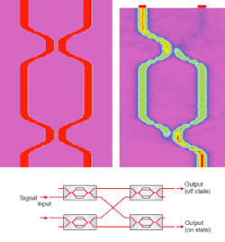
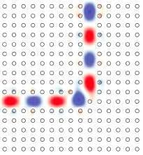
FIGURE 1. A Mach-Zehnder interferometer has two parallel single-mode waveguide arms running between a pair of coupling stages (top). Differences between the two arms (in length, temperature, or other characteristics) produce a phase shift that can cause constructive or destructive interference. The overlay color shows the path of light when the guides are adjusted to switch all light out of one port. Four of these interferometer stages can be combined to make a 2 ¥ 2 switch in the configuration shown (bottom).
Some serious technological limitations have slowed the pace of optical integration with planar waveguides. One is the inherently high attenuation of current planar waveguides, often measured in tenths of decibels per centimeter rather than per kilometer. Another is the long interaction lengths required to perform optical operations, typically millimeters or centimeters rather than the micrometer scales of integrated electronic components. Yet in practice the biggest limitation has been the lack of demand for integration. That market pressure is changing. Although sales have dropped, customer demand for lower costs is pushing manufacturers to consider integration to reduce production costs.
Interference effects
Most current waveguide devices fall into one of two very broad classes, depending on how they operate on light. One family relies on interference between light that is divided so it travels through two or more parallel single-mode waveguides, then recombined; examples include electro-optic switches and array waveguide multiplexers. The second depends on the interaction between light and the materials of the waveguide itself, such as amplifiers and electro-absorption modulators. Some other devices do not fall readily into either of these categories.
A broad range of waveguide devices is based on the generalized Mach-Zehnder interferometer configuration (see Fig. 1). Light from two inputs is mixed in a coupler and divided between two parallel waveguides. Light emerging from the two parallel guides is combined in a second coupler, which can split it between two separate outputs or deliver a varying intensity to a single output guide. The direction the light goes depends on how the light emerging from the two guides interferes.
Wavelength selectivity is possible if the two waveguide arms differ in length. The device is configured so constructive interference between light in the two parallel arms directs the light out one output port, while destructive interference directs it out the other. Because the two arms are unequal, constructive interference occurs only at certain wavelengths, where integral numbers of waves fit into both arms. At intermediate wavelengths, outputs from the two arms are 180° out of phase, and destructive interference directs the light out the other output port.
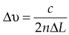
This principle is used in the interleaver, which directs alternating optical channels out of the two output ports. The interleaving shift Dn is a uniform increment in frequency (not wavelength), given by the equation
null
where DL is the difference in length. If the refractive index is 1.5 and the two waveguides differ by one millimeter, the frequency offset is 100 GHz.
Commercial interleavers normally are made from fibers in the same Mach-Zehnder configuration, but planar waveguides allow integration. At this year's Optical Fiber Communication Conference (Anaheim, CA), Manabu Oguma and colleagues at NTT Photonics Laboratories (Tokai, Japan) reported making compact planar waveguide interleavers with 50-GHz channel spacing. They developed a foldable design that packed three interleaving stages into a rectangular array only 4.2 cm long; the three stages would have stretched 20 cm if not folded.
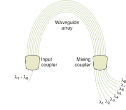
The waveguide array or array waveguide demultiplexer is based on an extension of this principle. Many parallel waveguides gather light from an input coupler, and deliver it to an output coupler. Differences in the waveguide lengths cause interference effects that, as in a diffraction grating, direct different wavelengths at different angles. Another set of output waveguides is arranged around the output coupler at the proper angles to pick up the desired wavelengths (see Fig. 2). A single passive monolithic array waveguide can demultiplex 40 or more optical channels, making it very attractive for systems with high channel counts.
Interferometric switches and modulators
The two-armed interferometer design also can be used in active devices, by operating on one or both arms of the interferometer to change their effective length, and thus the phase difference between them. Varying the phase shift between the two parallel arms modulates the output intensity continuously in a modulator. In switches, the phase shift jumps between two possible values, one directing the output out one port, the other out the other. Each switching element has only two inputs and two outputs, so the number of elements required increases with the square of the number of ports.
Traditional electro-optic modulators and switches are based on changing the voltage applied across waveguides in lithium niobate or III-V semiconductors, which modulates their refractive index and thus the phase shift between the arms. Typically the modulation voltage is applied with opposite polarity across the two guides, so a +V and -V modulation adds to an effective modulation voltage of 2V. Electro-optic modulation and switching are inherently very fast, but they require large surface areas, and lithium niobate devices are inherently polarization sensitive.
Another way to change the refractive index is by varying the waveguide temperature in thermo-electric devices. Temperature changes are on a millisecond time scale, inherently much slower than the electro-optic effect, and the refractive-index sensitivity means that operating temperature must be closely controlled. Thermo-optic switches have been developed in silica and polymers. Each switching element is relatively long, but they can be cascaded and wound around on a single substrate. For example, NTT has wound a device that otherwise would be 66 cm long so it fits onto a 10 ¥ 10.7-cm substrate.1
Developers are working on integrating different devices made from the same material subsystem. A silica array waveguide could, for example, be fabricated on the same substrate as a silica switching array, allowing the switching of demultiplexed optical channels.
Amplifiers and electro-absorption modulators
Amplifiers also can be fabricated in waveguide form, either by doping the waveguide with a light-emitting element—typically erbium—or by fabricating the waveguide in a III-V semiconductor that can produce gain. The amplification depends on the interaction between the light and the waveguide material.
Erbium-doped waveguide amplifiers operate on the same principles as erbium-doped fiber amplifiers, but differ in structures and applications. Erbium doping is higher than in fiber amplifiers, but waveguide amplifiers are much shorter, so their overall gain is lower. Most have been developed to provide wide-band gains in the 10-dB range for metro networks or other applications that do not need the full power of an erbium fiber amplifier. Alternatively, separate erbium waveguide amplifiers can be used for each of several optical channels, so amplification can be controlled separately on each channel.2 This can be important in situations in which some channels experience unusually high attenuation, as in add/drop multiplexers.
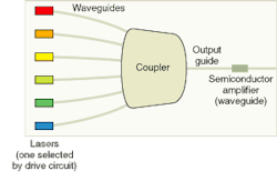
Standard semiconductor optical amplifiers also are waveguide devices, with the waveguide actually being the active stripe in the junction layer. They can readily be integrated with laser sources to boost output power. This is used in devices such as a multichannel tunable laser (see Fig. 3). A single wafer contains several lasers, each emitting at a different wavelength, and all feeding their output into a single waveguide N ¥ 1 coupler. In operation, the drive circuit selects only one laser; the others remain inactive. The optical amplifier compensates for the high coupler loss, raising overall output to the desired level.
Electro-absorption modulators are also semiconductor waveguide devices, so they can be integrated on a substrate with edge-emitting diode laser sources. The two have similar layer structures, but the modulator is a reverse-biased diode that transmits light when no voltage is applied, and absorbs light when a bias is applied.
A new type of semiconductor waveguide amplifier introduced last year by Genoa Corp. (Fremont, CA) at OFC 2001 embeds the amplifier stage within a vertical-cavity surface-emitting laser (VCSEL).3 Both devices share the same junction layer. Laser oscillation in the VCSEL is perpendicular to the junction, as in a standard VCSEL. The waveguide guides the amplified light horizontally in the junction layer in the region where the VCSEL oscillates. Combining the two devices gives level gain on optical channels through the erbium-fiber C-band, an important plus for multichannel optical systems.
Novel waveguide devices
New waveguide devices continue to emerge. Some are adapted from other fiber or optical components, such as a planar waveguide counterpart of the fiber Bragg grating, described at OFC 2002 by W. H. Wong and E. Y. B. Pun of the City University of Hong Kong. They wrote Bragg gratings with a 500-nm period onto the surface of a polymer waveguide deposited on an oxidized silicon wafer to make line filters for use in the 1550-nm window. They reported peak transmission better than 99% at the Bragg wavelength, with transmission of -27 dB. The 3-dB bandwidth was about 0.8 nm.4
Waveguides also can play important roles in emerging devices such as wavelength converters. Waveguides are used in delay lines and phase shifters to separate wavelengths in semiconductor optical amplifiers used as wavelength converters. Waveguides in nonlinear materials such as lithium niobate can be used for wavelength conversion.5
Flexible polymer waveguides are being developed as interconnection systems for optical devices. The waveguides are fabricated in a thin, flexible plastic sheet, which then can be used as the optical counterpart of an electronic wiring harness, to link optical subassemblies inside fiberoptic terminal equipment or switches. These waveguides can serve as couplers as well as links, and may eventually incorporate other optical functions.
In the long term, photonic bandgap materials look very attractive for planar waveguides that can bend, branch, and cross. The bulk of the photonic crystal blocks light propagation, while the waveguide contains defects that allow light to propagate through it. The light can theoretically turn a 90° corner with zero loss because it can propagate in the waveguide stripe, but cannot enter the surrounding zone (see Fig. 4). The concept has been extended to other devices, such as couplers, which split the input signal between two outputs. Research so far has been very encouraging, although fabrication of practical devices may prove challenging.6
Emerging prospects
Planar waveguide technology continues to mature. The first generation of electro-optic modulators and switches have long been standard products. A second generation of waveguide components has emerged in the past few years for multiplexing and switching, such as array waveguides. Some new devices have been introduced recently, both as discrete components, small-scale integration, and even for interconnection using flexible planar waveguides. But the most intriguing prospects are yet to come, with new concepts promising growing integration, particularly photonic crystal materials.
REFERENCES
- T. Goh et al., J. Lightwave Tech. 19, 371 (March 2001).
- J. Bristow, Laser Focus World 38, 101 (June 2002).
- D. A. Francis et al., OFC Postdeadline Paper PD13, (Anaheim; 2001).
- W. H. Wong and E. Y. B. Pun, OFC Paper TuC5, (2002).
- I. Cristiana et al., IEEE Phot. Tech. Lett. 14, 669 (May 2002).
- http://ab-initio.mit.edu/photons/index.html; .S. G. Johnson and J. D. Joannopoulos, Photonic Crystals: The Road from Theory to Practice (Kluwer, Boston, 2002).