Substrate-blind platform speeds photonic integration
Photonic-device designs often cannot be transferred between different platforms due to substrate-specific constraints, meaning that photonic-integration technologies on common substrates (CMOS on silicon or III-V optoelectronics on indium phosphide) are well-developed, while designs on unconventional materials like polymers, metals, or optical crystals are still in their infancy. But by using transition metal oxides and high-index amorphous chalcogenide glasses, researchers from the University of Delaware (Newark) collaborating with international researchers from the University of Central Florida (UCF; Orlando), Massachusetts Institute of Technology (MIT; Cambridge), the University of Texas at Austin, and the University of Southampton (England) have developed a substrate-blind platform that can tolerate deposition on a host of relevant substrates without requiring epitaxial growth and can be performed at temperatures <250°C.
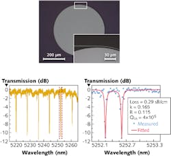
The substrate-blind integration process was demonstrated on three emerging substrate platforms: infrared (IR) optical crystals, flexible polymer materials, and 2D materials like graphene. The glasses were deposited on these substrates using thermal evaporation or solution-based processing and then patterned as waveguides, resonators, or gratings via photolithography or direct nanoimprinting. For microdisk resonators fabricated on mid-IR transparent calcium fluoride (CaF2) crystals and flexible polymer substrates, quality (Q) factors of 4 x 10⁵ and 5 x 10⁵ at wavelengths of 5.2 μm and 1550 nm were achieved—world records for planar mid-IR resonators and flexible resonator devices. Complex 3D structures can also be fabricated through sequential multilayer glass deposition and patterning. Reference: Juejun Hu, SPIE Newsroom, October 2014; doi:10.1117/2.1201410.005643.

