HIGH-VOLUME OPTICS FABRICATION: New technologies enable precise and cost-effective wafer-level optics
NIELS-CHRISTIAN ROMER HOLME, PALLE GELTZER DINESEN, ZIV ATTAR, STEVEN D. OLIVER and REINHARD VÖLKEL
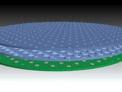
Widespread deployment of cameras in consumer products–most noticeably cell phones–has lead to a quest for improved cost efficiency in all manufacturing steps. Wafer-level manufacturing and assembly seems to offer a way forward for cost reduction. Whereas CMOS image sensors are already exclusively manufactured at the wafer level, this is not true for the lens stacks used in consumer cameras. There are a number of key challenges related to wafer-based manufacturing of camera lenses–including lens design, tooling, replication, metrology, and cost of ownership (see Fig. 1).
Efficient design
Although the basics of optical design for wafer-level cameras are similar to conventional optical design, a major change in approach is required to maximize the performance and yield of devices made at the wafer level. Typically, when designing optics, a statistical tolerance analysis determines expected yield, which ultimately dictates the price of the optics. When analyzing a wafer-level camera comprising one or more wafers stacked on top of an image-sensor wafer, a different approach is required for estimating and maximizing yields because, at the testing stage, disqualification of a lens means disqualification of an entire camera.
Tolerances are always important when designing optical systems but at the wafer level, the statistical nature of each tolerance and its consequences must be considered. Thus, when analyzing a wafer-level camera consisting of an image sensor and two lenses–each replicated on a wafer–a centering error between the two wafers will affect all the cameras extracted from the wafer stack. If such an error is large enough to degrade camera performance below specification, the resulting yield will be zero because all the lenses will suffer from the same centering error and performance degradation.
Another notable difference between conventional and wafer-level cameras is the inability to focus the camera after assembly. After mounting the lens stack on the image sensor, there is no assurance that the focal point of the optics will coincide with that of the image sensor, a condition that produces image blurring. The lack of focusing is dealt with partly by designing optics with an extended depth of focus–requiring use of a restoration algorithm after image capture–and partly by fine-tuning the thickness of the wafer nearest to the image-sensor wafer, which serves as a focusing spacer. The fine-tuning requires a one-time measurement of the actual focal point for each wafer stack.
Identifying the crucial tolerances, their impact, and their statistical behavior is key to optimum yields. While standard optical-design tools are very limited in their ability to control sensitivity to specific manufacturing or assembly errors, resulting in designs with high nominal performance but low yields, OpEra-Optics develops special tools and methods that are used to optimize optics for maximum production yields taking all manufacturing and assembly errors and their statistical behavior into account.
Tool manufacture
Any cost-effective technology for mass production of optics must rely on a cost-effective replication process–and for a replication process a master tool is required. If the replication tool does not meet quality requirements in terms of accuracy and finish, neither will the final lens. So tool manufacture is an important prerequisite for successful production of high-quality lenses. Wafer-level optics manufacture requires that the mastering technology be capable of making a tool that offers high form accuracy and surface finish of individual lens shapes; high reproducibility of lens shapes across a large wafer tool; high positioning accuracy of the individual lenses on the wafer tool; and highly aspheric, high-NA lenses with large sags.
Several tooling technologies can meet these requirements, including etching, and ultraprecision machining combined with a step-and-repeat replication into a final wafer-master. While etching offers very high accuracy and good surface finish, it is limited in the maximum sag and the deviation from spherical that can be accomplished. Ultraprecision diamond-turning of insert pins certainly offers the versatility to create complex geometries with large sags. The subsequent step-and-repeat process to create a wafer tool, however, is time-consuming and delicate.
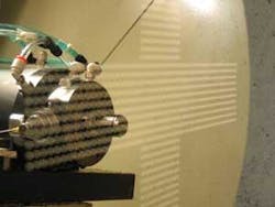
At Kaleido Technology we have implemented and customized an ultraprecision diamond-milling process, based on the use of a multi-axis ultraprecision machining system, a high-precision milling spindle, and ball-nose diamond-milling cutting tools capable of generating surfaces with optical finish (see Fig. 2).1 The milling process generates a large number of identical aspheric lens shapes sequentially across the wafer.Challenges associated with meeting the requirements for accurate wafer tools are mainly related to the prolonged machining time and dynamic instabilities of the machining system. Manufacturing a 200 mm wafer tool with 2000 lenses, as an example, can take as long as 120 hours to complete, and to maintain a high form accuracy and lens pitch accuracy, the machining system must be customized for extraordinary thermal stability. Minimizing the machining time requires pushing the dynamics of the machining process to the limit, and only through compensation for the associated instabilities can the form accuracy be maintained at the required level.
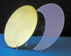
Properly addressing these challenges has enabled the machining of a monolithic wafer replication tool, populated with thousands of aspheric, high-NA lens cavities, each with form accuracy better than 0.2 µm (PV), lens position accuracy better than 3 µm absolute across the entire wafer and an excellent optical surface finish (less than 5 nm, root mean squared; see Fig. 3).Replication
Besides the tooling there are other challenges that must be addressed before large-scale deployment of wafer-level replicated lenses will succeed. Perhaps most important, the lens must be reflow- compatible, meaning that it must withstand a temperature of 240°C to 280°C for about two seconds, allowing for mounting of the camera module during the same process as the electronic components of the cell phone. In addition, the lenses must be resistant to UV light, sunlight, humidity, and hot-cold cycles.
The optical properties of the lens material are also important, and this is currently one of the key obstacles of polymer-based wafer-level optics. Available materials have limited refractive index and Abbe number, thus restricting the ability of cameras to compensate for chromatic aberrations and temperature-induced focus shift.
Microlens imprint lithography is an important technology that meets the above requirements.2 The hard tool manufactured with the aforementioned diamond-milling process is transferred into a soft PDMS (polydimethylsiloxane) stamp, which can then be used as the final replication tool for mass production. In the imprint lithography print, droplets of a liquid-polymer material are distributed on a glass base substrate. Then the soft tool is used to force the droplets to take the shape of the soft stamp, and a UV curing process “stiffens” the droplets forming a negative copy of the soft-tool lens shape.
A benefit of the imprint lithography process is that it can be carried out on a modified mask aligner (such as the Suss MA8 mask aligner capable of 200 mm replication of lenses) that is typically used in semiconductor manufacturing.
For efficient camera designs, bi-aspheric lenses must be used. This adds to the requirements for the replication process: in addition to the lens form and position (pitch) accuracy requirements outlined for the tool manufacturing, the imprint equipment must also be capable of double-sided replication with a small tolerance on the front- and backside lens center-to-center position.
Metrology
The metrology of optical lens systems must deal with both the characterization of each of the lens elements and the image quality of the final lens system. Traditionally each of the refractive surfaces of a lens element is characterized for form accuracy by means of a profilometer–most commonly, a noncontact, white-light-interferometer-based system, or a contact-stylus profilometer.
An interferometer-based profiler works well for spherical lens elements with shallow angles. However steep aspherical profiles that are common in today’s miniature lens systems are a problem. More advanced systems have recently adopted a stitching algorithm with a high numerical aperture (NA) objective that helps alleviate this, although there are still severe limitations on the profiles that can be characterized. A contact-stylus profilometer works equally well for shallow and steep aspheres. But a problem with this approach is that the stylus usually leaves a mark on the surface of the lens under test, especially in soft polymer lenses that are typical in low-cost imaging systems. An additional drawback is that a 2-D scan of the surface cannot adequately capture the accuracy of the complete 3-D surface (such as problems characterizing astigmatism).
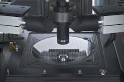
Advances in optical metrology equipment especially wavefront-error characterization have been made. One example is wavefront-error characterization based on a Shack-Hartman approach. This system utilizes a dense array of microlenses to focus the wavefront onto a CCD imaging sensor. The deviation in the spot location for each lens is recorded and the aberrated wavefront is characterized. Then the Zernike coefficients are extracted and compared to the original lens prescription. This technique is suitable for wafer lens characterization because the testing time for each lens is relatively fast and the objective can be rapidly positioned to each lens on the wafer (see Fig. 4).Finally, it should be noted that advances in automated systems have enabled fully automated, large-scale wafer-scale characterization of the modulation transfer function, an important standard for determining final lens-system performance.
Total cost of ownership
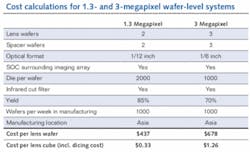
Cost of ownership calculations involve determination of the overall cost of manufacture by estimating throughput, process costs, yields, and so forth, that affect the overall cost of building the final product in production. These calculations for wafer-level camera modules involve multiple dependant factors that significantly affect the final number. A simplified wafer optics replication, stacking, bonding, singulation, and testing process serves to illustrate the results using a 1.3- and 3-megapixel wafer-level lens system (see table).The cost-of-ownership model is a valuable tool. Once the model is established, a variety of different scenarios can be compared to determine the best cost. For example, manufacturing location, new vs. used tools, comparisons of different yields, optical formats, comparison of different suppliers, materials, and so on, can all be compared. Furthermore, an analysis of each process step can be evaluated in a pareto format to determine which step is more significant in the overall cost of the lens unit–from this the areas where development and manufacturing optimization are needed can be identified.
REFERENCES
- N.C.R Holme et al., Proc. SPIE 7062 (2008).
- M.T. Gale, Ch. 6 in Micro-Optics: Elements, Systems and Applications, H.P. Herzig, Ed., Taylor and Francis, London (1997).
Niels-Christian Romer Holme is chief technology officer and Palle Geltzer Dinesen is chief sales officer at Kaleido Technology, Ryttermarken 15-21, DK-3520 Farum, Denmark. Ziv Attar is chief executive officer at Opera Optics, POB 10149, Zikron Yaakov, Israel 30900. Steven D. Oliver is a private consultant at So-Semi Technologies, 1460 Rosecrest Terrace, San Jose, CA 95126; e-mail: [email protected]. Reinhard Völkel is chief executive officer at Suss MicroOptics, Rue Jaquet-Droz 7, Ch 2000 Neuchatel, Switzerland; e-mail: [email protected].
