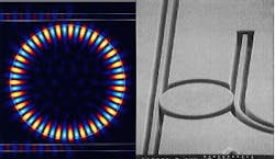
Two groups of researchers have developed integrated waveguiding ring and disk resonators that show promise as versatile elements for optoelectronic integrated circuits. In postdeadline papers (CPD22 and CPD23) presented at the Conference on Lasers and Electro-Optics in May the groups described strongly waveguiding rings and disks that can act as narrowband tunable filters. The resonating rings—analogous to resonators used in electronics and microwave devices—could be used as filters for wavelength-division multiplexing and as integrated optical switches or modulators.
Although the structure of the ring and disk waveguides was first proposed by a researcher at Bell Laboratories (Holmdel, NJ) in 1969, the technology required to make such devices for optical use has not been available until now.1 Both optical lithography and electron-beam lithography were used by the researchers to make devices with feature sizes of 0.5 µm, and in some cases as small as 0.1 µm. The lithographic techniques used were developed for microelectronics processing, which means other electronics fabrication techniques also could be applied to making the small optical integrated devices, with consequent cost reductions as production quantities increase.
Both ring and disk devices confine the light within the waveguide by etching material away from around the waveguide—a large change in the refractive index between the waveguide and air occurs at the boundary, which does a good job of trapping light inside the waveguide. The confinement is good enough that waveguides with relatively tight bends can be made with less bending radiative loss than structures with a smaller change in refractive index between the waveguide and surrounding material.
In the structures, light is injected into a straight 0.5-µm-wide waveguide. A ring or disk of the same waveguiding material is formed close to the straight waveguide, such that the evanescent mode of light at certain wavelengths couples into the ring or disk from the first waveguide, and the light couples out of the waveguide on the other side. At the resonant wavelength of the ring or disk, the structure can couple much of the power out of the first and into the second waveguide (see figure). The resonant wavelengths are dependent on the diameter of the ring and propagation speed of light in the waveguide.
Current work
Both groups of researchers fabricated devices on semiconductor substrates. Jim Foresi, Brent Little, and others at the Massachussetts Institute of Technology (Cambridge, MA), Kanagawa Academy of Science and Technology (Kawasaki, Japan), and Hewlett-Packard (Palo Alto, CA) used polycrystalline silicon (Si) on silicon dioxide (SiO2). Deana Rafizadeh, Jian-Ping Zhang, Seng-Tiong Ho, and others at Northwestern University (Evanston, IL) and Cornell University (Ithaca, NY) made structures from indium gallium arsenide (InGaAs) on gallium arsenide (GaAs) substrates.
The MIT group’s silicon devices were processed at Hewlett-Packard’s ULSI Research Laboratories (Palo Alto, CA) using optical lithography. The waveguide consists of a 0.5-µm-wide polycrystalline silicon layer, bordered by air, that rises 0.2 µm above the isolating SiO2 layer that is deposited on a silicon substrate. The group grew rings with diameters as small as 6 µm and demonstrated a free spectral range of 25 nm at 1540 nm with a Q factor of 250. The Q factors expected of the device are much higher, but the waveguides and ring in the sample were fused due to the resolution of the lithography used to make the device. The fusion led to added scattering at the junctions. Little says, "Practical Qs of more than 1000 can be expected." Even with the fused section, 95% of the light from the input waveguide was transferred to the output waveguide.
The AlGaAs/GaAs devices, including both ring and disk resonators, were made by the Northwestern researchers at the Cornell Nanofabrication Facility using electron-beam lithography. The waveguide is a submicron-thick layer of GaAs on AlGaAs, etched to a depth of 2.2 µm. The rings and disks of diameters 10.5 and 20.5 µm were etched, as well as tightly curved waveguides. Gaps between the waveguides and resonators were 0.1 µm wide. The loss in the disk resonator was less than that of the ring because there was no scattering loss from the inner waveguide rim—in a disk, as opposed to a ring, there is no inner rim. The 10.5-µm-diameter disk resonator yielded a Q of more than 8500 at 1500 nm and a free spectral range of 21.6 nm with a linewidth of 0.18 nm.
The silicon-based resonator could be integrated with electronics. Many current electronics and microwave circuit resonator applications, explains Foresi, could be optically implemented by these rings.
The Northwestern group has previously made a photonic-wire laser with a submicron cavity coupled to a waveguide (see Laser Focus World, Aug. 1995, p. 24); the researchers hope to integrate the resonators with the laser and, by adding electrical contacts, to create tunable filters and modulators in an integrated device.
REFERENCE
1. E. A. J. Marcatili, Bell Syst. Tech. J., 2071 (1969).
