
Photomasks are the fundamental component of optical lithography, the element that actually produces the pattern projected on the wafer. Manufacturers typically use electron-beam lithography followed by a wet-etch process to pattern a 1000-Å-thick layer of chrome on a fused silica substrate. The substrate standard is now 6 × 6 in. by 0.25 in. thick, but will soon shift to 9 × 9 in. (see photo).
The industry is currently hustling to address manufacturing requirements for fabricating masks for the 0.25-µm chip generation at 248 nm. Looming not far behind is 193-nm lithography, which places even more stringent requirements on substrate quality, writing processes, and pattern inspection and repair. Although some of the technical base for 248-nm lithography will carry over, some scientists in the photomask community see a daunting challenge for the industry. "Masks are a problem at 193 nm," Microlithography World's Marc Levenson, a pioneer in photomask technology, says flatly. "The technology is late. [Manufacturers] are going to try to use methods that would have been good at 0.25 µm for the subsequent generations. At feature sizes for 0.15- and 0.18-µm lithography, transfer becomes nonlinear, errors are magnified."
Materials still the issue
As with projection systems, bulk optical materials are a fundamental issue for mask manufacturers. Defects in the quartz substrates must be smaller than the minimum feature size of the mask. Steppers for 193-nm lithography will be 4X reduction (meaning that features on the photomask will be four times as large as those on the wafer), but they still place high demands on substrates and substrate inspection systems. With the planned shift to 9 × 9-in. substrates, the problem becomes greater.
"The real killer is glass anomalies, which are unrepairable," says Bob Gesullo of Hoya Corp. (San Jose, CA). Still, he notes evidence that the quartz used today is feasible for the 193-nm generation. "There's some debate, but most of the recent work done by quartz suppliers suggests that present quartz could be used." Blank preparation presents difficulties, however—flatness specifications tighten as minimum feature size shrinks. The current flatness standard for 0.25-µm chips is 2 µm, but it will drop to 0.5 µm for subsequent generations. Mask thickness requirements simultaneously limit the amount of material that can be removed to achieve this flatness.
Assuming adequate substrate defect control, chrome and fused silica can be used for binary masks at 193 nm. More-advanced techniques, such as phase-shift masks in which varying layer thicknesses impart resolution-enhancing phase delays in the illumination wavefront, face complications. Few materials offer the necessary transmission control at 193 nm. "When we went to 248 nm, we could use the same materials as for longer wavelengths," says Bruce Smith of the Rochester Institute of Technology (Rochester, NY). "We've pushed them as far as we could. For 193 nm, we'll have to go to new materials."
Smith and his group are investigating various metallic oxides and nitride combinations to develop materials that give the needed phase/ transmission properties. Such new materials complicate mask production. "You have to be able to pattern them," says Smith. "Not only do you need the optical properties, you need the materials to be process compatible."
Inspection and repair
Unlike semiconductor manufacturers, who can think in terms of percent yield on a wafer, photomask manufacturers must guarantee a zero-defect product. Thus mask inspection and repair are as important as the writing process itself. Most inspection work is done at twice the lithographic wavelength, even though mask professionals concede that this technique might conceivably miss features that would print through in the lithographic process. Moreover, inspection takes place beyond the resolution limit of the system, and sophisticated computer algorithms are required to compare gray levels and isolate defects.
"We`d like to move to 193-nm inspection," says Jim Wiley of KLA (San Jose, CA), "but we`re not able to implement until low-cost and reliable CW sources become available." For 193-nm reticles, inspection systems will be based near 248 nm, perhaps at 257 nm (frequency-doubled argon-ion laser). "We haven't yet started a program to inspect at 193 nm."
Defects, once identified, must be repaired, most commonly by gallium-focused ion beam. The instrument can remove excess chrome and reconstruct films where flawed. Not unexpectedly, at 193 nm the process becomes more difficult. During the ion bombardment, the beam implants gallium into the mask substrate, reducing transmission. Decreasing beam intensity is not necessarily an answer. "We don't even know if we can do images or process work using a limited number of ions," says Dianne Stewart of Micrion (Peabody, MA).
In addition, the tight tolerances of photomasks for the 0.18-µm and subsequent generations may exceed the capabilities of beam control. The masks are nonconductive, while the beam is positively charged. This generates a charged particle imbalance at the mask surface that can shift the position of the ion beam, compromising repair accuracy. Moreover, the ion beam sputters faster at the edges of features, so that repair processes can create trenches around the repair site. With phase-shifted masks, says Stewart, "the problem triples, quadruples. When you have damage regions at interfaces, they act as little phase shifters." Micrion is investigating gas-assisted etching chemistries, as well as novel beam-scanning strategies to improve repair at interfaces.
Laser defect repair is an alternative, but thermal damage can again cause transmission loss. At 248 nm, laser repairs to quartz substrates create transmission losses of roughly 10%. Losses would be higher at 193 nm, creating an excessively large transmission differential between repaired and unrepaired regions. To address this issue, Mark Linden of laser repair tool manufacturer Quantronix (Hauppauge, NY) says the company plans to shorten pulse durations of its Ti:sapphire regenerative amplifier-based repair system from the nanosecond regime to the picosecond regime.
The clock is ticking
Last year the semiconductor industry required about half a million photomasks; by the year 2000, that number is estimated to reach 1.2 million. Even assuming only 5% to 10% of those masks are for 193-nm lithography, the numbers are still huge. Whether produced by electron-beam lithography or by laser writing, masks are serially written, and according to most industry experts, these processes are simply not fast enough. Vector-based versus raster-based writing systems may offer faster production, but they require more initialization time.
Indeed, time appears to be the primary concern all around. "The killer is the calendar," says Marc Levenson. "Everything that needs to be done can be done and could have been if we'd started five years earlier." On a laboratory level, processes are capable of meeting demands. The difficulty will be bringing the technology to production level on schedule. "The photomask industry has a full plate right now," says Hoya's Bob Gesullo. "These are exciting times."
Photoresist: Better living through chemistry
Photoresist is a polymer deposited on a wafer that allows integrated-circuit manufacturers to actually create the circuit pattern on the wafer. When exposed to the proper wavelength of light and developed, photoresist (typically 0.5 µm thick) undergoes a solubility change. The developer renders an exposed positive photoresist more soluble and renders an exposed negative photoresist less soluble. Thus the development process dissolves the exposed positive resist and leaves the original unexposed positive resist in place on the wafer. The converse occurs with a negative photoresist, leaving the opposite tone pattern. These patterned photoresists function as templates for subsequent processing steps such as etching (see figure).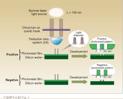
The shift to 193-nm lithography requires an appropriate family of resists, material that will allow light to penetrate all the way through the applied layer so that it will react correctly in the subsequent development bath, adhere to the wafer substrate, and withstand etching steps. Conventional resins and resist materials contain aromatics that strongly absorb 193-nm light, making them unsuitable. Chemists are trying to engineer a resist that offers a high degree of photosensitivity to 193-nm illumination, while remaining robust to etch processes. Ideally, these new resists would be compatible with the developers used in current generations.
The principal challenge, notes Robert Allen of IBM Almaden Research Center (San Jose, CA), is defining a polymer system that is the central platform people build resist upon. With both i-line and 248-nm lithography, researchers established the primary platform early on and merely worked on variations of those polymers. At 193 nm, resist chemists have yet to establish that backbone. "That's the central problem and also what makes this field so incredibly interesting," Allen says. "There are many different ways to skin a cat."
Top two materials
The two primary contenders for resist materials are polymethacrylates and cyclic olefins. In a situation reminiscent of Goldilocks and the Three Bears, cyclic olefins offer tremendous etch resistance but little photosensitivity, while polymethacrylates are highly photosensitive but have insufficient etch resistance. Like Goldilocks, resist chemists are on the hunt for the variation that is just right, providing good etch resistance and adequate photosensitivity. Beyond etch resistance, researchers contend with issues such as environmental stability and compatibility with conventional developers.
There is also concern about resist aspect ratios. Some studies have suggested that an increase in photoresist aspect ratio as feature sizes drop will cause resist patterns to become unstable. Resist features might draw together with surface tension in dense regions or break off the substrate altogether. Some researchers, like Don Hofer of IBM Almaden, dismiss this issue. "The problem of lines falling over and effects of surface tension in developers are not significantly different at 193 nm than they were at 365 and 248 nm." Others, like Roderick Kunz of MITLL are more conservative. "What I've seen is that I`ve been able to do decent lithography in the 0.15- to 0.17-µm range, so I`m not convinced that aspect ratio will be categorically a problem." It may not be as easy as that, he continues. "I fear that it will be okay in the development lab, but problems will occur when it goes to production."
If surface tension in developers is an issue, surfactants may compensate, but there is resistance in industry to use the surfactant-containing resists. Thinning the resist layer is not necessarily an option, as that decreases etch robustness. This would increase the pressure to create an etch-resistant material.
The coherent light used in 193-nm lithography generates standing-wave patterns within the resist, so antireflection coatings must be applied to substrates prior to the resist. With the technical background gained in developing antireflection coatings for 248-nm lithography, however, most resist chemists do not expect antireflection-coating development to be a problem.
Thin-film imaging
Most researchers agree that the single-layer resists will be there on time, but express concern about bilayer resists and materials for advanced techniques such as thin-film imaging, necessary to extend 193-nm lithography out as far as it will go. In one thin-film imaging approach, the stepper patterns a 1500-Å-thick layer atop a thicker resist layer. An oxygen reactive ion etch (RIE) process transfers the image from the thin-film layer to the resist layer below. This approach reduces the demands on the exposure system because it requires a minimal depth of field, so smaller features are printable.
"The whole field of thin-film imaging at 193 nm is behind the progress in single-layer resins," says Don Hofer of IBM Almaden. "A considerable amount of R&D is required to produce a manufacturable 193-nm thin-film imaging material/process. Some of us believe that the bilayer form of thin-film imaging will be superior to top-surface imaging because line-edge roughness may not be so prominent. However, bilayer resists require completely different chemistry from single-layer resists because a significant amount of silicon must be incorporated in the resist."
The resist community as a whole is a scene of furious activity. Researchers at IBM Almaden developed the first 193-nm single-layer resist. A polyacrylic-based resist intended purely for tool and process development, it offers high sensitivity but little or no etch resistance. Researchers at Bell Labs recently reported a cyclic-olefin-based single-layer resist that appears promising (see Laser Focus World, June 1997, p. 13). Japanese companies like NEC, Fujitsu, and Hitachi, as well as Korean companies like Samsung, are also doing promising work. The resist community seems confident that the issues will be resolved in time for the deployment of 193-nm production-line steppers, and they appear to be right.
ACKNOWLEDGMENTS
A number of people were very generous with their time, offering me information, material, and contacts as I compiled this report. They include John Shamaly (SVG Lithography); Roderick Kuntz, David Shaver, and Mordechai Rothschild (MIT Lincoln Laboratory); Wayne Pantley (Alpine Research Optics); John Bruning (Tropel); Marc Levenson (Microlithog- raphy World); Jim Wylie (KLA); Elsa Reichmanis and Omkaram Nalamasu (Bell Laboratories).
Also Larry Bond (DEC); John Peterson (Sematech); Mark Linden (Quantronix); Larry Thompson (ISI); Bruce Smith (Rochester Institute of Technology); Greg Hughes (Dupont Photomasks); Dianne Stewart (Micrion); Bob Gesullo (Hoya Corp.), Robert Allen, Don Hofer, and Carl Larson (IBM Almaden Research); John Wiesner (Nikon Precision); Dave Markel (Ultratech Stepper); Katherine Derbyshire (Solid State Technology); and Gary Forrest (SensorPhysics).
About the Author
Kristin Lewotsky
Associate Editor (1994-1997)
Kristin Lewotsky was an associate editor for Laser Focus World from December 1994 through November 1997.