Semiconductor manufacturers look to short wavelengths
Optical lithography is the primary method for bulk manufacture of integrated circuits. In optical lithography, a photomask is back-illuminated and imaged onto a photoresist-covered wafer. The resist undergoes chemical changes as a result of the exposure, and after it is developed, portions remain on the wafer to protect regions from subsequent processing steps such as etching, ion implantation, and metallization. This sequence is iterated up to 35 times to produce a typical chip.
As the demand continues for ever-faster computers and more-powerful processors, manufacturers are forced to increase the density of elements on a chip. Density, however, is limited by minimum printable feature size. Although the lithography community has developed a repertoire of optical tricks to print subwavelength-scale features, successive generations of chips have driven source wavelengths from 436 nm (mercury g-line) to 365 nm (mercury i-line) and below. The 0.25-µm chip generation relies on deep-UV 248-nm lithography (krypton fluoride excimer laser), which most experts expect to also produce the first 0.18-µm devices. For the 0.15-µm generations and beyond, however, the industry looks to 193-nm lithography.
A feverish development effort is underway to achieve all of the elements necessary to bring production-level 193-nm lithography on line by 1999. Optical materials for projection systems pose one of the biggest challenges. Most materials are highly absorptive at 193 nm and undergo optical damage; fused silica, the primary material for this wavelength, suffers from compaction effects that can introduce phase errors over time, degrading image quality. In the wafer plane, a whole new class of photoresists are required that are simultaneously highly sensitive to illumination and highly robust in etch conditions. Defects in photomask substrates can impact patterning, and repairs with current technology typically degrade 193-nm light transmission. Some optical designs in steppers require highly stable, line-narrowed argon fluoride (ArF) excimer laser sources with high repetition rates and tight pulse-to-pulse energy control (see Laser Focus World, June 1997, p. 89).
The challenges are daunting, but researchers and manufacturers have made significant progress. Nearly ten years ago, the Defense Advanced Research Projects Agency (DARPA) awarded funds to the Massachusetts Institute of Technology Lincoln Laboratory (MITLL; Lexington, MA) to identify the major issues in 193-nm lithography and begin developing technologies to bring that generation of steppers to reality. SEMATECH, an industry consortium initially funded in part by DARPA, is now organizing the US effort to insert 193-nm technology into production. In Japan, the Association for Super-Advanced Electronic Technology (ASET) was formed for the same purpose.
Pressing for time
The timeline for 193-nm system deployment is considered aggressive. "It takes 18 to 24 months to integrate [the technology] into a process," says Joe Langston of Intel (Santa Clara, CA). "If you need it in 2000 for a pilot line, you need resists and optics by mid-1998, and it looks like that might not happen." Most industry insiders agree that optimized 248-nm systems will produce the initial devices in the 0.18-µm chip generation.
"Some manufacturers will start with 193-nm systems at 0.18 µm, but most will stretch the 248-nm technology," says John Shamaly, vice president of technology at Silicon Valley Group Lithography (SVGL; Wilton, CT). "193 nm will probably come in on the 0.15-µm and 0.13-µm generations." Some researchers, like David Shaver of MITLL, believe that 193-nm systems will be able to produce chips in the 0.1-µm generation.
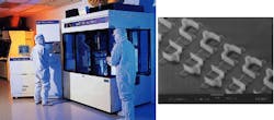
Stepper companies are pushing hard to bring the technology to fruition. Integrated Solutions Inc. (ISI; Tewksbury, MA) has produced nine small-field steppers for photoresist development (see photo opposite page, top), and SVGL has already delivered a full-field prototype system to MITLL for use in process development and testing (see photo, left). According to Shamaly, SVGL expects to release full-field (26 × 33 mm) pilot production-level systems by the end of 1998, with general deployment to follow in 1999. Other stepper manufacturers, such as Nikon Precision (Belmont, CA), are actively working on full-field steppers, but projected release dates are not available.
Clearly 193-nm lithography is expected to be fully deployed at the turn of the century and will play a pivotal role in the future of semiconductor manufacturing. The challenges exist, but solutions are emerging, thanks to the work of researchers worldwide. And perhaps in the year 2000, I'll find myself back at the keyboard, writing a Special Report entitled "X-ray lithography—life after DUV."
About the Author
Kristin Lewotsky
Associate Editor (1994-1997)
Kristin Lewotsky was an associate editor for Laser Focus World from December 1994 through November 1997.