Micro-patterned bull’s-eye improves SERS sensitivity
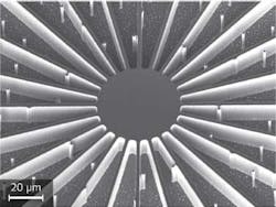
To maximize the number of molecules delivered to the detection area of a substrate when performing surface-enhanced Raman spectroscopy (SERS), researchers at Harvard University (Cambridge, MA) and the École polytechnique fédérale de Lausanne (EPFL; Switzerland) have developed a micropatterned bull’s-eye structure that uses superhydrophobic (water-repelling) action. That is, a water droplet containing gold colloids, for example, is attracted to the bull’s-eye center, concentrating the colloids as it dries. Later, analyte molecules delivered via another water droplet adhere tightly to the colloids, increasing the number of molecules probed in a small area and correspondingly magnifying the SERS signal. For example, Rhodamine 6G can be detected at molar concentration levels as small as 10-15.
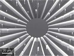
Rather than using expensive electron-beam lithography (EBL) and focused-ion-beam (FIB) milling methods, the SERS bull’s-eye was fabricated in silicon using simple optical lithography. A hexagonally oriented array of micropillars (3 μm radius, 15 μm height) spaced 20 μm apart is interspersed among 24 radial microfins with the same dimensions but length of 2 mm to create the 4-mm-diameter superhydrophobic structure with a 50-μm-diameter circular platform at the center. A water droplet is pinned in the center based on Cassie–Baxter modeling equations that deliver optimized contact angles for the patterned and smooth surfaces of the silicon substrate. The method significantly improves SERS sensitivity while simultaneously reducing the amount of gold needed to perform a SERS measurement. Contact Wuzhou Song at[email protected].

