Two-photon process cures hybrid polymers into photonic-crystal lattices
Lattices of inorganic-organic hybrid polymers designed as photonic crystals have been achieved with resolutions down to 100 nm. Ruth Houbertz and others at the Fraunhofer Institute (Wuerzburg, Germany) with Boris Chichkov and others at Laser Center Hannover (Hannover, Germany reported their findings at the Nanotech 2004 conference in Boston in March.1 The researchers achieved these high resolutions by using two-photon absorption to polymerize the material, offering a direct-write technology that can create 3-D structures quickly. This is a step toward using these materials as photonic crystals.
The researchers have been developing this process for several years, but in addition to reporting the finer resolution at Nanotech they reported large-scale processing of areas up to 270 × 270 µm using two-photon polymerization.
Hybrid polymers
The polymers incorporate an inorganic backbone of silicon oxide silicon. Various organic groups that attach to the backbone can be chosen to tailor materials properties—including index of refraction, optical absorption losses, thermal expansion, and transparency. Ruth Houbertz's group at the Fraunhofer has been working with one specific class of trademarked materials ORMOCERs. The materials are produced by sol-gel synthesis and have adjustable refractive index (from 1.45 to 1.6), high optical transparency with low loss at 830, 1330, and 1550 nm, good thermal and mechanical properties, and low cost.
"You can tailor the physical and chemical properties related to the specific requirement," says Houbertz. "For example for low optical losses and refractive index, for dielectric properties (such as very low dielectric losses up to the gigahertz regime or passivation against environmental influences such as humidity), or hydrophobicity/hydrophilicity."
The inorganic backbone provides more thermal stability than most organic materials that are being developed for the purpose. For example, ORMOCERs are stable up to 415°C, whereas PMMA softens in the range of 80°C to 115°C. These photo-patternable materials are also compatible with semiconductor processing, and can be coated on many different substrates.
Compared to commercial acrylate systems, ORMOCERs also offer better surface quality. In general, the inorganic backbone of ORMOCERs inhibits the material from parasitic polymerization.
Two-photon polymerization
The ORMOCER can be patterned using standard UV lithography, but two-photon polymerization allows users to pinpoint the volume to be polymerized with precision—and in three dimensions. The precursors are designed to polymerize when exposed to two photons, rather than the more conventional single photon. The chances of a single molecule absorbing two photons at the same time is high where the optical intensity is high, but falls off quadratically as the intensity falls.
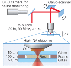
Boris Chichkov's group at Laser Center Hannover used a Ti:sapphire femtosecond laser beam emitting at 780 nm focused through a high-numerical-aperture lens into the volume of a liquid resin (see Fig. 1). Users control the location of polymerization in the x-y plane by scanning and in the z plane by changing the focal distance of the beam. Where the laser focus moves through the resin, the material is polymerized. Just as in conventional (single-photon) UV lithography, nonirradiated resin can be dissolved in a solvent and removed. A final UV exposure finishes curing of the remaining material.
The threshold behavior and nonlinear nature of the two-photon polymerization process and thus a resolution beyond the diffraction limit can be realized by controlling the laser pulse energy and the number of applied pulses.
Because the optical losses of ORMOCERs are lower than 0.2 dB/cm at data wavelengths and 0.5 dB/cm at telecommunication wavelengths, this microstructuring technique is attractive as a way of fabricating micro-optics, including lens arrays for fiber coupling, integrated-waveguide devices, and photonic crystals.
The researchers used the method to fabricate a regular 3-D lattice such as would be used for a photonic crystal (see Fig. 2). The structure was built up from individual rods with a diameter of about 200 nm, spaced 450 nm apart. The total fabrication time was about five minutes.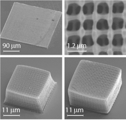
Challenges
Several challenges still must be overcome before the material can be used for photonic crystals at near-IR wavelengths.
When photosensitive resins crosslink, they shrink. While this isn't a problem in the bulk of the polymer device (because each volume pixel shrinks to the same extent and remains exactly at the position of the controlled laser focus), it does cause distortion near the interface with the substrate when the final UV exposure process occurs.
The final shrinkage can be reduced by using more laser power during the initial polymerization. The researchers are investigating this, as well as altering the model of the structure to compensate for shrinkage near the interface.
The final hurdle to writing fast, cheap, photonic crystals at telecom and datacom wavelengths is to increase the refractive index. "We are currently tuning the material toward a higher refractive index in order to achieve real 3-D bandgap materials," Houbertz says.
Reference
- R. Houbertz et al., Proc. Nanotech 2004, NSTI, paper MO31.06.