Arrays of holes launch surface plasmons
If a metal surface is properly structured, it can take incoming light and convert it to surface plasmons (which are oscillations of free electrons at the metal's surface); likewise, it can convert surface plasmons to freely propagating light. Someday, photonic circuits may contain elements made of metal structures, with surface plasmons traveling from one structure to the next. Such circuits would contain components with familiar names—Bragg gratings and photonic crystals, for example—yet would be far smaller than today's optoelectronic integrated circuits.1 Giving impetus to the creation of these circuits, researchers at the Université Louis Pasteur (Strasbourg, France) and the Université de Bourgogne (Dijon, France) are launching plasmons with microgratings consisting of arrays of holes in metal film, then converting the plasmons back to light.
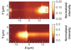
Using a focused ion beam, periodic rectangular arrays of holes are created in 150-nm-thick gold films deposited on glass. In one example, two arrays are created on the same substrate, one to create plasmons from light and the other to reconstitute the free-space light. Both gratings have a 760-nm period and 250-nm holes; the gratings are separated from each other by 30 µm. The smaller, 11 × 11 source array (top, seen at right) receives the light, converting it to plasmons, which travel leftward. A larger, 41 × 41 probe array (seen partially at top left, and almost in its entirety at bottom) converts the plasmons back to light.
The source array is excited by light at normal incidence from a Ti:sapphire laser that is focused to a 10-µm-diameter spot (half-cone angle of 8°). To visualize the phenomenon, the researchers use a photon-scanning-tunneling microscope, which reveals the conversion of plasmons to light at the probe array. Between the arrays, the plasmons are almost invisible due to the lack of outcoupling, but fringes can be seen (bottom), showing that the plasmons are also bouncing back and forth between the arrays and interfering with each other. Rotating the polarization of the incoming laser light by 90° sends the plasmons in the y instead of the x direction.
The results show that the surface plasmons do not spread much as they travel, which bodes well for future surface-plasmon integrated circuits. One of the researchers, Thomas Ebbesen of the Université Louis Pasteur, notes that start-up companies are already forming to capitalize on surface-plasmon technology—for example, Spectalis (Nepean, Ont., Canada).
REFERENCES
- William L. Barnes et al., Nature 424, 14 (August 2003).
- Eloise Devaux et al., Appl. Phys. Lett. 83 (Dec. 15, 2003).

