Submicron photolithography opens new areas of holographic design
Enabled by advances in deep-ultraviolet photolithography and computer-based holographic design, a new family of transport devices is emerging. This use of volume-holographic structures within a planar waveguide is being called integrated holographics.
The development of new tools often generates new opportunities. From the juggernaut of electronics fabrication comes the emerging ability to produce planar diffractive structures with 100-nm pixelation and centimeter-scale spatial coherence. Deep-ultraviolet (DUV) photolithography, the hero of electronics fabrication, has evolved to performance levels needed to directly or indirectly-for example, by creating masters for nanoimprinting-produce high-resolution and coherent structures in quantity and at low cost.
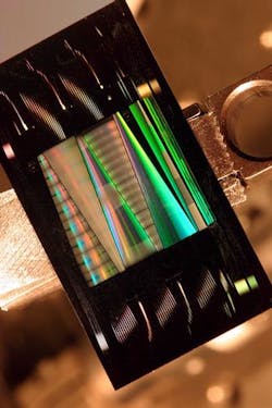
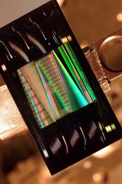
FIGURE 1. Integrated holographic structures can be lithographically scribed and etched onto the core layer of a silica-on-silicon planar waveguide. This structure spans much of the DUV stepper’s 20 × 20-mm field. Channel waveguides direct signals from off-chip and launch them into the wedge-shaped holographic designs where they are filtered and focused into output-channel waveguides. Some structures provide multichannel spectral filtering; others provide multiplexing for coarse and dense wavelength-division multiplexing. To enhance visibility of the etched structures, the upper cladding was not applied.
Although DUV photolithography was not developed with photonics (or nanophotonics) in mind, the implications in this area are profound-especially in relation to holography and its applicability to planar waveguides. Numerous devices and photonic-circuit approaches are now made possible by application of new lithographic capability to computer-designed volume holograms produced in planar waveguides (see Fig. 1). These lithographically scribed planar holograms provide a unifying technological approach to multiple photonic-circuit functions-including spatial routing, focusing, wavefront matching, flexible spectral filtering, optical-pulse shaping, and temporal correlation-based signal processing-some of which are currently difficult to integrate and require discrete devices such as thin-film filters or fiber gratings. Emerging fabrication technology also provides for cost-effective scribing of planar holograms onto highly stable and robust planar-waveguide materials such as silica and various semiconductors.
Creating volume holograms in waveguides
A simple hologram represents an interference pattern between two optical beams, which are commonly referred to as object and reference beams. A thin hologram is an interfacial sampling of the interference pattern wherein each point on an incident wavefront interacts with one or a few fringes. Conversely, thick or volume holograms span a depth dimension along the propagation direction of incident optical beams so that each point on an incident wavefront interacts with multiple (perhaps many thousand) interference fringes. The hologram can create a complex output wavefront (recreate an object beam) in response to irradiation by an input beam with a wavefront that duplicates a simple reference beam. This elemental holographic property is used in three-dimensional (3-D) image storage. More generally, holographic structures can efficiently transform input signals in a variety of ways useful in photonic-circuit applications such as in collimating and focusing beams.
A volume-holographic structure can become highly selective as to which input signals it will interact with. A spatially extended volume hologram can be essentially noninteractive with an input signal unless its wavefront and wavelength falls within narrow ranges. This wavefront/ wavelength selectivity can be used in various ways, including the design of powerful integrated multiplexers and spectral filters, or as a basis for photonic integrated circuits (ICs) in which signal streams freely cross and overlap but are still subject to this selective control.
Holographically mediated signal routing and control differs from the typical electronic-style photonic transport in which wire-analog channel waveguides are used, subject to maximal bending rates and significant proximity constraints. Holographic-transport approaches solve many of the same problems addressed by photonic-crystal waveguides, but can exhibit lower losses and polarization sensitivity through use of smaller refractive-index contrasts. Holographic structures with high-index contrasts can be used, however, if signal localization is important.
While holographic principles can provide powerful function and device advantages, their implementation has been constrained by a lack of flexible and cost-effective fabrication means. Interferometric and other past approaches to holographic fabrication do not measure up to the task of implementing general designs. Interferometric fabrication, for example, requires the use of writing beams similar to those that will interact with and be controlled by the desired holographic structure. In a complex circuit scenario, such beams are impractical to construct prior to implementation of the circuit. In 3-D, volume-holographic fabrication is still dependent on interferometric means, but in planar waveguides the situation has dramatically changed. With the combination of DUV photolithography at 250-nm-and-finer resolution, planar waveguides, and computer-based volume-holographic design, it is finally possible to create an entirely new breed of optical ICs and devices.
A typical planar waveguide consists of three transparent dielectric layers: a central higher-index-guiding (or core) layer, and two cladding layers-all mounted on a substrate. In silica-based media, the core can be 2 to 6 µm thick, while cladding layers can be 10 to 15 µm thick. Holographic diffractive structures can be photolithographically scribed onto one of the core-cladding interfaces via familiar etch-and-deposition methods. As mentioned above, such structures act as volume holograms to core-bound signals and can thus be designed to provide both spectral filtering and wavefront morphing capability for certain input signals while at the same time exhibiting near-transparency for nontargeted signals. The technology associated with lithographically scribed volume-holographic structures in planar waveguides is being called “integrated holographics.”
Fabricating integrated holographic devices
Many discrete devices can be designed and implemented in the context of integrated holographics. These include high-performance spectral filters and wavelength multiplexers. For example, an integrated holographic spectral filter can be created in which light enters from an input channel waveguide and expands in the slab waveguide, interacting with a family of curvilinear diffractive contours (see Fig. 2). The contour spacing is equal to approximately half the in-medium wavelength (Bragg resonance condition). For a 1.5-µm wavelength in a silica-based waveguide, the spacing will be approximately 0.5 µm, indicating an etched feature size of 0.25 µm. An etch depth aspect ratio of 1:4 (etch depth 1‑µm in this example) can be achieved. Each contour is weakly reflective and optimally reshapes the input signal so as to enter the output port.
FIGURE 2. In a holographic-Bragg-reflector (HBR) filter, light enters through an access channel, expands in the 2-D core waveguide, and then interacts with the scribed volume hologram. A spectrally filtered or time-coded output beam is created that can be optimally matched (via holographic imaging) into an output access channel waveguide. Detailed control of position and amplitude of individual contours via computer design and lithographic fabrication provides powerful spectral filtering and pulse shaping. The upper cladding was not applied to enhance visibility of the etched structures.
The spectral-transfer function of the volume hologram is determined by the amplitude and relative phase of each diffractive contour, which can be precisely controlled via computer design, mask generation, and photolithographic projection. Differential phase shifts consistent with fabrication via binary etch processes can also be introduced to generate amplitude control.
Another device is referred to as a holographic Bragg reflector (HBR) and is described as an integrated fiber Bragg grating or an integrated thin-film filter.1 Unlike fiber Bragg gratings, HBRs have separate input and output ports. Like fiber Bragg gratings and thin-film filters, HBR filters can be designed with a broad range of spectral-transfer functions. In fact, the precise line-by-line amplitude and phase-control lithographically available provides a pathway to finely structured spectral-transfer functions. An HBR filter can be keyed to complex molecular spectra for substance detection or provide tailored passband devices for communications applications; resolutions of 5 to 10 GHz have been demonstrated. On the other hand, reflective bandwidths spanning hundreds of nanometers can be implemented with appropriate diffractive-contour refractive-index values. Filters with very high bandwidth/resolution ratios in the thousands should be possible.
The wavelength and wavefront selectivity of volume holograms allows multiple HBR filters to be placed on a single die to function as multichannel spectral filters or as wavelength demultiplexers. In a demultiplexer, signals of differing wavelengths enter through a single input port. The input port is coupled via multiple wavelength-selective HBRs to wavelength-specific output ports (see Fig. 3). Holographic Bragg reflectors can occupy distinct spatial regions of the waveguide or they can be collocated and interspersed. Compared to arrayed waveguide grating (AWG)-based multiplexers, the integrated holographic multiplexer is typically smaller, providing more die per wafer and smaller device footprint. Also, the central passband wavelength and passband profile of the channels are independently and flexibly configured without the insertion-loss penalties found in the case of AWGs.
As a holographic device, HBR filters and multiplexers are essentially immune to point fabrication defects. Polarization sensitivity can be made extremely small through use of low refractive-index contrast and appropriate design and annealing of internal waveguide structure. Dominant polarization effects tend to be wavelength shifts of a few gigahertz in well-designed silica-on-silicon units.
The HBR filters and multiplexers are based on simple retroreflective geometry and signal interaction with a single holographic structure. In photonic circuits based on holography, optical signals flow from source to destination in slab-waveguide environments through interactions with a series of holographic structures, each of which provides spectral and wavefront conditioning as the signals are relayed from one structure to the next.2 Such holographic structures (and routed/ processed signals) can overlap extensively. The complete structure is fabricated in a single photolithographic step using a laser-written reticle scribed with the entire complex computer-generated volume-holographic structure.
Such photonic-transport fabrics combined with even-order grating structures to send or receive signals off-slab provide a powerful approach for integrating photonic transport into electronic-circuit designs and for implementing optical-interconnect functions. While the principles behind photonic-transport fabrics based on volume-holographic structures have been known for some time, it is only with the emergent nanofabrication capability of modern reduction photolithography that such concepts can be cost-effectively utilized.
Looking to the future, integrated holographic structures may be implemented in a variety of channel and slab waveguide environments consisting of any guiding material including polymers, silica, silicon, or general semiconductor materials. In some cases, very low-cost devices may be produced by nanoimprint-based device replication. One can expect powerful advances to follow in integrated holographics now that it is finally possible to fabricate almost any designed planar structure and to do so in robust, stable waveguide environments.
REFERENCES
1. C. Greiner, D. Iazikov, and T. W. Mossberg, J. Lightwave Technology 22(1) 136 (2004).
2. T. W. Mossberg, C. M. Greiner, and D. Iazikov, Optics & Photonics News 15(5) 26 (2004).
THOMAS W. MOSSBERG is chief technology officer, CHRISTOPH M. GREINER is a senior scientist, and DMITRI IAZIKOV is a senior design engineer at LightSmyth Technologies, 860 West Park St., Suite 250, Eugene, OR 97401; e-mail: [email protected].


