Mask inspection rises to the subwavelength challenge
As wafer fabs transition from 248-nm optical lithography to 193 nm and beyond, reticle-inspection systems are adopting sophisticated image-enhancement techniques to keep pace.
As semiconductor-wafer fabs transition from 248 to 193 nm and beyond, photomask and inspection-tool developers are scrambling to ensure their products follow suit. The reticle is the master used to print the wafers and therefore a single missed defect can result in millions of dollars of waste. With reticles becoming more complex and design rules dropping below 90 nm, mask-inspection systems must be able to detect traditional defects that can print upon first use and progressive defects that can worsen over time and jeopardize device yield.1
"The goal of lithography is to produce an integrated circuit that works," said Scott Hector, mask strategy program manager for the lithography division of International Sematech (Austin, TX). "The mask contains the master pattern for the integrated-circuit layers, and you want the mask pattern to be perfect in advance so you can be sure it will do its job in the litho process and not affect the yield of the ICs in the wafer fab."
Photomasks hold microscopic images of electronic circuits on quartz plates, and photolithography transfers these circuit patterns onto wafers to form integrated circuits. Defects on the mask are reflected on the wafer; as chip complexity increases, so does the difficulty in detecting errors. The masks are typically inspected with a scanning laser system or a microscope after the absorber material has been patterned. A defect is any flaw affecting the geometry or critical dimension and can cause the circuit not to function. The customer will indicate the size of defects that will affect its process; all defects that size and larger must be repaired or the mask will be rejected and rewritten. There are currently three main mask-inspection methods: die-to-database, in which the mask image is compared to the design data; die-to-die, in which the images of identical dies within a mask are compared; and contamination, in which the mask is checked for non-pattern-related defects.2
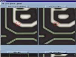
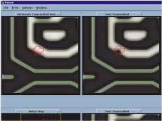
Certain types of defects are harder to detect in smaller-feature resolution patterns than others (see Fig. 1). Today the types of defects that can be present on a reticle include opaque (unwanted chrome or molybdenum disilicide [MoSi2]), clear (missing chrome), particles, partially transparent films, scratches, electrostatic discharge damage, microfissures in or polishing grooves on the quartz, transmission loss from repair, and subpellicle crystal growth. As a result, most mask shops and fabs now require several types of defect-detection systems (see Fig. 2).
"For us, the inspection of our final product is very critical," said Curt Jackson, engineering manager at DuPont Photomask (Austin, TX). "We have multiple inspection systems from multiple suppliers, starting from mature technologies (using 488 nm) that we use for the 0.25-µm technology node and for 0.18-µm inspection. In the 130-nm node, we have transitioned to the 364-nm inspection wavelength, which is the workhorse tool in the inspection industry today. We are inspecting to capture defects down to 100 nm in size, and the inspection-tool suppliers have done some unique things to allow us to capture defects that are one-third the size of the inspection wavelength."
Current mask-inspection systems use short wavelengths and high-magnification optics to detect defects down to 100 nm in size. Mask-inspection wavelengths have progressed from 400 to 500 nm to around 200 nm, which is currently considered state of the art. According to Jackson, while the wafer industry's workhorse tool is the 248-nm system, photomask inspection wavelengths historically lag behind wafer fab stepper-tool wavelengths. In addition, photomask systems typically operate at feature sizes four times larger than those found in the wafer fab systems.
"In general, photomask inspection-tool suppliers have relied on the massive R&D that has gone into the wafer tools to pave the way," Jackson said. "But they have also been pretty creative in finding ways to capture defects that are a fraction of the wavelength and enable a nearly 100% capture rate for the 100-nm defects. Still, at this point we are looking at photomasks with feature sizes four times that of the wafer, which means the line width on the photomask is four times larger than the patterns that print on the wafers."
Image enhancement techniques
With the push to put more and more capabilities on each semiconductor, chip designers are turning increasingly to subwavelength lithography to print features down to 65 nm in size; this means working below the diffraction limit, where the optics cannot faithfully reproduce the desired pattern without using resolution-enhancement techniques. For example, the 90-nm technology generation uses 193-nm light for patterning. At the 90-nm generation, transistor features are less than half the wavelength of the patterning light. This trend, in turn, has led to other developments that can affect the mask over time, such as crystallization and radiation contamination.
"It is very important to understand the challenges in mask inspection today," said Anja Rosenbusch, who is responsible for applications and customer relations in the mask inspection unit at Applied Materials (Rehovot, Israel). "The big challenge for users is to inspect masks of 248 and 193 using the 365 system. Also, the mask itself is getting very complicated. The number of critical layers is increasing. These layers are built with advanced masks, which use enhancement techniques to enhance the area image."
Several techniques have been developed to enable subwavelength patterning, including off-axis illumination, pattern-specific resists, phase-shifting masks, and optical proximity correction (OPC). According to Rosenbusch, an industry favorite is OPC, in which the photomask is modified to compensate for diffraction effects that occur during subwavelength patterning. Because of various optical effects associated with imaging the mask pattern onto the wafer surface, proximity effects can distort the pattern; these effects can be compensated for by making changes in the mask pattern such as line edge placement and subresolution features. Over the past decade OPC has evolved from simple rule-based algorithms to the complex model-based OPC used today. This trend has placed additional burdens on mask and inspection toolmakers because OPC patterns are susceptible to their own defects. Because the OPC features are small, their fidelity is not as good as the main features, which emphasizes the tradeoff between collecting all defects and reducing the number of nuisance defects.
Another key enhancement technique is phase-shift masks, in which the light from adjacent features undergoes phase inversion to increase contrast and enhance resolution. Device line widths have become so narrow (0.18 µm and below) that conventional light sources and lenses, and/or binary photomasks cannot ensure the designs print accurately on the wafer. Although designs can be built on ordinary binary masks, the lines blur together when reduced onto the wafer. Even utilizing the most advanced lithography equipment available, the device's individual feature sizes are so small or so close together that they no longer resolve without some technological improvement. Phase-shift masks enhance contrast to expose the photoresist and print features at resolutions that binary masks are unable to achieve with current light sources and lenses. DuPont has developed several phase-shift-mask approaches, including embedded attenuated phase-shift masks and alternating-aperture phase-shift masks.
"The embedded phase-shift mask came into widespread use with the 248-nm wafers," Jackson said. "Now as we shift down to 90 and sub-90-nm design rules, we are seeing a lot more alternating or etched-quartz hard-phase-shift masks. This approach allows us to take advantage of the phase information in the light to further enhance contrast. But it also creates an obvious challenge in mask inspection because you have to account for any defect created in the etch process. The subresolution features that wafer designers are designing are on the order of the smallest features we can reliably detect. So we also struggle with methods that can detect these aberrations. You can see it, but not always capture it in a single inspection run."
Another challenge for inspection-tool developers is mask error-enhancement factor (MEEF), in which errors in the critical dimensions are not transferred to the wafer in direct proportion to the optical reduction value of the lithography system; that is, a defect on the mask can be quite small but translate into something quite large on the wafer. In the low-k1 area (k1 is a constant in the equation that relates critical dimension [CD] to wavelength and numerical aperture), the MEEF becomes a significant problem, as it consumes a larger than anticipated percentage of the critical-dimension tolerance budget. As a result, mask CD uniformity requirements have been tightened significantly to find MEEF-related CD defects prior to the first printing at the wafer fab. The challenge for mask-inspection methodology lies in the fact that conventional mask inspection detects defects according to their dimensions on the mask, but MEEF-related CD defects are often caused by CD deviations close to metrology resolution.
Bridging the gap
One potential solution to MEEF and other issues associated with phase-shifting is to bridge the wavelength gap that has historically existed between inspection systems and wafer-production systems—that is, to build mask-inspection tools that operate at the same wavelengths as the wafer fabs. But this is much easier said than done.
"There is a growing debate over whether a mask should be inspected at the same wavelength as the exposure wavelength used in wafer manufacturing," Hector said. "The desire is to continually shrink the wavelength and hopefully catch up with the wafer fab wavelength, but it makes everything more difficult. The systems are not as powerful at shorter wavelengths, the optics have to withstand new radiation effects, the detectors have to be created for shorter wavelengths. . . . The result is that inspection-system design becomes more complicated."
Even so, all of the mask-inspection suppliers are developing and testing lower-wavelength systems (currently 193 nm). According to Rosenbusch, the only way to ensure that a phase-shift mask will operate cleanly in a production environment is to inspect the mask at the same wavelength with which it was created. In addition, at 193 nm there is the issue of crystal growth, stemming from some of the organic materials used to clean the surface of the masks interacting with the laser radiation. Here again, Rosenbusch says, it is very difficult to see these crystals unless the inspection tool is operating in the same wavelength as the stepper.
Beyond 193, the inspection-tool challenges become even greater, however; for example, with the chromeless phase-shift mask the opaquing film is eliminated, so that the mask is printed only with phase information, meaning there is almost no contrast, only the phase edge. And the push to move into the extreme-UV will be a tremendous challenge for the mask-inspection tools because of the feature sizes and the use of reflected-light photomasks.
"The challenge for inspection-tool suppliers is to find lasers that have the desired short wavelengths and proper coherence properties, both spatial and temporal," Hector said. "Also, because these tools are expected to run 24/7, laser reliability is very important. And when you go to the shorter wavelengths, you have to manage all the high-energy radiation effects on the optics, both in the laser itself and in the inspection tool optics."
REFERENCES
- Yield Management Solutions Mag.3(1) (Autumn 2000) www.kla-tencor.com.
- S. Hemar, A. Rosenbusch, and R. Falah, OE Magazine (February 2004).


