Photonics firms fill semiconductor niches
As the semiconductor industry continues to push toward smaller feature sizes and linewidths, optics and laser manufacturers are also continuing to develop process and metrology technology to meet the new challenges. This trend was evident at the annual Semicon West meeting in July, at which more photonics companies than ever were on hand, working to make further inroads into one of the healthier high-tech industries around these days. Semicon West was split into two segments: the wafer-processing segment was held in San Francisco, CA, July 12–14, while the final-manufacturing segment met in San Jose, CA, July 14–16.
Newport (Irvine, CA) was touting the addition of elastomeric material to its vibration and isolation systems to significantly improve horizontal stability over traditional isolation-system designs and meet the increasingly precise positioning needs of semiconductor processing and metrology. According to Tom Miller, director of product marketing for optics and optomechanics, Newport, in its first foray into lithography objective lenses, is also collaborating with researchers at the Massachusetts Institute of Technology (MIT; Cambridge, MA) to develop a "hyper-numerical-aperture" immersion lens with a numerical aperture of 1.3 for feature sizes down to 50 nm. The lens is based on a fluorinated fused-silica material to get around the birefringence issues associated with calcium fluoride.
New Focus (San Jose, CA) displayed beam-stabilization systems based on mounts and picomotors specifically designed to withstand harsh environments with deep-UV and x-ray radiation, very high vacuums, and total submersion (for immersion lithography), according to Aaron Van Pelt, product-line manager.
Photolithography is one of the most challenging areas for Coherent Molectron (Portland, OR), according to Sean Bergman, product manager for power and energy products. And development of power and energy metering technology to meet those needs often provides technology for further development in other application areas. Pulse-repetition rates for photolithographic laser light sources are currently moving from 4 kHz to 6 kHz, he said, which has driven the development of electronics for metering systems toward system-sampling rates between one and two orders of magnitude faster than the current pulse repetition rate.
Semiconductor-microelectronics applications such as via drilling and memory repair also need such rapid sampling, particularly for UV-laser technology, Bergman added. So the company is currently working to adapt technology developed for photolithography into a reasonable market range for the much more cost-sensitive microelectronics market. Another major push is in developing immersion-lithography energy-measurement systems that will function in wet environments with very-high-numerical-aperture optics.
JPSA Laser (Hollis, NH) announced an upgrade to its UV-DPSS (diode-pumped solid-state) laser wafer-dicing system to handle 6-in. gallium arsenide and silicon wafers. The company has been shipping both excimer and UV-DPSS laser systems to customers in Japan since the second quarter of 2004 and is currently negotiating further system sales to the Japanese market, according to Jeffrey Sercel, JPSA president. Cognex (Natick, MA) announced pattern location and alignment enhancements to its geometric pattern-matching software to facilitate wafer alignment and metrology tasks. These advances include locating barely visible objects or patterns in grainy or faint images produced by high-magnification techniques such as scanning-electron microscopy, and performing partial match alignment for processes such as defect detection in which only a portion of the desired pattern is available in an image.
Cymer (San Diego, CA) introduced an excimer light source designed to support 45-nm immersion lithography, which is also the third generation of the company's master-oscillator power amplifier (MOPA)–based argon fluoride laser series and is expected to begin shipments in the first quarter of 2005. Cymer also begins shipments this month of its 4-kHz krypton fluoride excimer light source, originally announced last February for sub-100-nm design nodes.
Laser-induced ultrasound
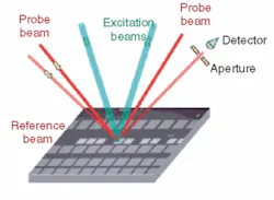
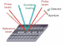
Philips Advanced Metrology Systems (AMS; Natick, MA) is continuing to launch an innovative approach to metal-film-thickness metrology based on the generation and measurement of laser-induced ultrasound waves using diode-pumped microchip lasers (see figure). The installed base of laser-induced-ultrasound metrology systems is composed primarily of femtosecond Ti:sapphire lasers, according to chief technologist Michael Gostein, who hopes to increase market share for the AMS technique based on the compactness and cost advantages of microlaser technology.
On the imaging side, Coreco Imaging (Montreal, Canada) set up a Vision Lab in its booth, bringing together applied machine-vision experts and members of Coreco Imaging's development team to give OEM design engineers the opportunity to discuss pressing machine-vision application issues with specialists in vision algorithms, image acquisition, and applied machine-vision-system processes. "This was an opportunity to take a close look at the latest machine-vision technology and to learn how new advances are meeting the demands for increased inspection throughput," said Philip Colet, vice president of sales and marketing. According to Colet, Coreco's high-speed vision processors are used for wafer, flat-panel, and plasma-discharge inspection applications where very high-speed acquisition and processing throughput is required.

