Short-wavelength 3-D photonic crystal is laser-written
Micro-optical components based on photonic crystals (PCs) promise to become useful as microcavities, mirrors, switches, and routers, each on a scale of a few wavelengths in size. To realize practical devices, it is necessary to have full control of the lattice parameters of PCs over an appropriate volume. A major goal is to create structures that prohibit light propagation in a designated wavelength range in any direction so that, for example, microcavities can be made that have an outcoupling surface freely definable by an appropriate local change of the lattice. Diamond-like structures, for one, fulfill this condition.1
Various approaches to creating 3-D (volume) PCs have been tried, including holographic exposure of photoresists. In this method, several beams from a laser irradiate the resist under appropriate angles so that an intensity pattern is generated because of interference in the volume. When further processed, the resist forms an air-material lattice or, when infilled with a different material, a lattice of two materials with different indices of refraction. But creating the desired face-centered-cubic (fcc) lattices requires beam-propagation angles within the resist that are difficult to achieve.
To get around this problem, a group of researchers at the University of Karlsruhe and the Forschungszentrum Karlsruhe (both of Karlsruhe, Germany) have designed a corner-cube prism that was used for the incoupling of four laser beams.2 Without the prism, the required angles are beyond reach as a result of refraction of the beams at the air-photoresist interface. The four beams were obtained from a single-mode frequency-tripled Nd:YAG laser supplying 8-mJ pulses of 6-ns duration at 355 nm. Each beam could be controlled with respect to polarization and intensity. The researchers chose a thick-film resist (SU-8) made by MicroChem (Newton, MA) that shows low absorption in the near-UV and no change in index of refraction during exposure. Post-baking and developing the resist resulted in a nearly fcc lattice with a lattice constant of 550 nm, which showed a distinct transmission reduction to about 13% at 680 nm.
Direct laser writing
A different approach, direct laser writing (DLW), offers full freedom in lattice design and introduction of locally different geometries. In this manner, the Karlsruhe researchers, together with groups from the University of Central Florida (Orlando, FL) and Iowa State University (Ames, IA), manufactured an fcc lattice by moving a photoresist sample on a piezoelectric three-axis scanning stage across the focused beam of a 120-fs 800-nm Ti:sapphire laser, the repetition rate of which could be varied from single shot to 1‑kHz.3 The group again used SU-8 resist so that the technique would remain compatible with and complementary to holographic lithography.
In this case, two-photon-absorption processes were required for polymerization. In DLW, the beam must be focused very sharply to realize sufficiently tiny structures. Two-photon polymerization takes advantage of the nonlinear response of the resist by which the threshold for polymerization is increased, which is only achieved in a narrow region around the geometric focus. In this way, layers spaced 500 nm apart and with an in-plane rod spacing of 1.5 µm had already been achieved elsewhere.4 These photonic crystals had indeed shown optical stop bands in the IR and even at telecommunications wavelengths, although at those wavelengths only in second order. In addition, lattice shrinkage and distortion had deteriorated the quality of the lattice.
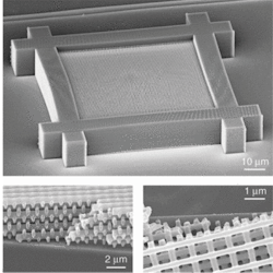
In contrast, the group of German and American researchers demonstrated almost perfect fcc lattices by two-photon DLW, the lattice being spanned by a solid frame preventing bending and distortion (see figure). The 40-layer device measured 100 × 100 mm, and the lattice within 70 × 70 mm. The rods were built up by joining individual “voxels” of ellipsoidal shape, the size of which could be controlled by the single-pulse energy of the laser. The lateral rod diameter could be controlled from 180 to 250 nm. Subsequent layers of parallel rods were rotated by 90° such that rods in every other layer were parallel again, but shifted by half a period. Thus, the unit cell of the fcc crystal consisted of four layers of rods. The massive surrounding wall was made by the same technique.
To generate photonic bandgaps in the telecommunications wavelength region between 1.5 and 1.3 µm, samples of different rod spacings from 1 to 0.8 µm were made of 24 layers each. Pronounced transmission dips were achieved that shift through the 1.7- to 1.3-µm range as the rod distance was decreased.
REFERENCES
1. M. Maldovan, E. L. Thomas, Nature Materials 3(9) 593 (2004).
2. Yu. V. Miklyaev et al., Appl. Phys. Lett. 82(8) 1284 (2003).
3. M. Deubel et al., Nature Materials 3(7), 444 (2004).
4. M. Straub, M. Gu, Optics Lett. 27(2) 1824 (2003).

