METAMATERIALS: Kinetic inductance produces negative refractive index as low as -700
While conventional optical metamaterials can exhibit a negative index of refraction, it doesn’t reach any lower than the negative single digits. In contrast, researchers at the Harvard School of Engineering and Applied Sciences (SEAS; Cambridge, MA), collaborating with the Weizmann Institute of Science (Rehovot, Israel), have demonstrated a drastically new way of achieving negative refraction in a metamaterial that results in a negative index as low as -700.1
Kinetic inductance arises from Newton’s second law
The underlying physics of previous work in this field has often involved magnetic inductance. The research group instead explored kinetic inductance, which is the manifestation of the acceleration of electrons subjected to electric fields according to Newton’s second law of motion.
The researchers’ change in strategy stems from a simple shift in ideas. “Magnetic inductance represents the tendency of the electromagnetic world to resist change according to Faraday’s law,” says principal investigator Donhee Ham, a researcher at SEAS. “Kinetic inductance, on the other hand, represents the reluctance to change in the mechanical world, according to Newton’s law.”
“When electrons are confined perfectly into two dimensions, kinetic inductance becomes much larger than magnetic inductance, and it is this very large two-dimensional kinetic inductance that is responsible for the very strong negative refraction we achieve,” says lead author Hosang Yoon, a SEAS graduate student. “The dimensionality profoundly affects the condensed-matter electron behaviors, and one of those is the kinetic inductance.”
Semiconductor interface is where it happens
To obtain the large kinetic inductance, the researchers base their device on the creation of a 2D electron gas (2DEG), which forms at the interface of two semiconductors—gallium arsenide (GaAs) and aluminum gallium arsenide (AlGaAs; see figure). The very pure 2DEG sample used in this work was fabricated by coauthor Vladimir Umansky of the Weizmann Institute.
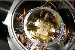
Ham’s team sliced a sheet of 2DEG into an array of strips and used microwaves to accelerate electrons in the strips on one side of the array. The resulting movements of electrons are detected by the strips on the other side of the array, where electrons are consequently accelerated. The proof-of-concept device propagates an effective wave to the right in a direction perpendicular to the strips, each of which acts as a kinetic inductor because of the electrons’ acceleration therein. This effective wave exhibited what the researchers call a “staggering” degree of negative refraction.
The primary advantages are the ability to localize electromagnetic waves into ultra-subwavelength scales and dramatically reduced size. This concept demonstrated with microwaves, if extended to other regions of the electromagnetic spectrum, could prove important for operating terahertz and photonic circuits far below their usual diffraction limit and in the near-field. It may also one day lead to extremely high-magnification microscopes and new forms of optical tweezers.
For now, the device operates at temperatures below 20 K. The researchers note that a similar result can be achieved at room temperature using radiation in the terahertz range, which Ham’s team is already investigating, with the carbon structure graphene as an alternative 2D conductor.
REFERENCE
1. H. Yoon et al., Nature, 488, 65 (Aug. 2, 2012).
About the Author
John Wallace
Senior Technical Editor (1998-2022)
John Wallace was with Laser Focus World for nearly 25 years, retiring in late June 2022. He obtained a bachelor's degree in mechanical engineering and physics at Rutgers University and a master's in optical engineering at the University of Rochester. Before becoming an editor, John worked as an engineer at RCA, Exxon, Eastman Kodak, and GCA Corporation.

