Integrated devices make an optical bench on a chip
Integrated devices make an optical bench on a chip
Batch-mode lithographic fabrication methods produce free-space micro-optical bench components on a chip.
Ming C. Wu, L. Y. Lin, S. S. Lee, and C. R. King
Free-space
integrated optical systems, in which photons propagate freely in space between optical elements, have many applications in optical interconnection, image processing, sensing, display, and data storage systems. Building a micro-optical system on a silicon chip is an intriguing idea; such an approach can greatly reduce system size and weight. Guided-wave methods have been implemented, such as silicon optical benches on which silica waveguides on silicon substrates link optoelectronic devices and silicon wafer boards that incorporate fiberoptic arrays. These guided-wave devices, however, are not suited to free-space optical systems.
Realization of a free-space micro-optical bench is challenging for several reasons. First, it requires integratable free-space optical elements. Though systems composed of separately produced elements installed in alignment holes on a silicon substrate are feasible, monolithic, batch-fabricated free-space optical elements are preferred. Second, because multiple-element cascading requires a system optical axis parallel to the substrate, and because free-space beams are usually expanded to diameters of several hundred micrometers, very tall three-dimensional optical elements are needed. Such components are not compatible with conventional planar fabrication techniques of silicon processing.
Third, on-chip optical alignment capabilities must be available. Integrated micropositioning stages are needed for optical alignment, switching, or scanning. Micromachined movable structures such as micromotors must be integrated with the optical elements.
Advances in integrated micro-optics
Our group at the University of California (UCLA, Los Angeles, CA) has successfully developed free-space micro-optical bench designs in which three-dimensional, free-space, micro-optical elements and movable micro-mechanical elements are fabricated on the same wafer using batch processing techniques.1 As in conventional systems constructed on laboratory optical tables, the free-space micro-optical bench includes passive optical elements (lenses, gratings, beamsplitters, filters, and so forth), micropositioners (translation stages or rotation stages), and active optoelectronic components (photodetectors and laser or LED sources).
Unlike conventional systems, however, free-space micro-optical bench systems are micron-scaled and batch-fabricated on silicon substrate. Because the micro-optical elements on a free-space micro-optical bench are precisely placed by photolithography, they can be prealigned during photomask layout. To compensate for fabrication tolerances, fine optical alignment is performed with on-chip micropositioners.
Surface-micromachined micro-hinge technology was first developed by Kris Pister, now of UCLA.2 This process allows optical elements to be made by conventional planar microfabrication techniques, then folded into three-dimensional structures (see Fig. 1). Elements are patterned on a polysilicon plate that sits on top of a sacrificial silicon dioxide (SiO2) layer. A hinge pin is defined at the bottom of the optics plate. The pin is first covered by another sacrificial SiO2 layer and then anchored to the substrate by a polysilicon staple. Once the SiO2 is removed, the optics plate can freely rotate out of the substrate plane.
The lens angle is precisely fixed by a lens mount consisting of two alignment plates made by the same surface-micromachining processes but folded orthogonal to the lens. The
2-?m-wide groove at the end of the V-shaped opening firmly locks the position of the lens. This mount also enhances the mechanical strength and stability of the lens plate.
Optical elements from 10 ?m to a few millimeters in size can be produced by this technique; elements as tall as 1.3 mm have been realized. For example, our group has fabricated a
180-?m-diameter micro-Fresnel lens with a 500-?m focal length and an optical axis 254 ?m above the substrate. The lens displays good optical performance, collimating the output from a single-mode optical fiber to a 0.33! divergence angle.
High performance notwithstanding, the micro-Fresnel lens is a diffractive optical element and suffers from low efficiency. For optimal performance, a micro-optical refractive element is required. We have successfully fabricated an out-of-plane spherical microlens by combining a reflow technique with surface-micromachining technology (see Fig. 2). When heated to 200!C, photoresist on the surface-micromachined lens OreflowsO into a spherical shape, in this case with a 406-?m radius of curvature.
The 300-?m-diameter lens has demonstrated excellent optical performance, collimating single-mode fiber output to a divergence angle of 0.15!. Focal length is 645 ?m, and the lens is 30 ?m thick at center. Maximum deviation from spherical is below 0.5 ?m to within 5 ?m of the edges. The optical axis is photolithographically fixed to the same height as that of the other micro-optical elements in the system.
An example of movable micro-optical elements is a tunable Fabry-Perot bandpass filter for wavelength division multiplexing (WDM) applications (see Fig. 3). To form the filter, we applied three pairs of Si/SiO2 dielectric layers as mirrors on both sides of a 1.6-?m-thick vertical polysilicon plate, obtaining a finesse of 14. The angular position of the filter is tuned with an integrated rotation stage to yield a tuning range of 58.5 nm at an operating wavelength of 1.3 ?m.
Element alignment and beam steering
Micro-optical elements and active optoelectronic devices in the free-space micro-optical bench can be prealigned during the design and fabrication process. In one demonstration system, a semiconductor edge-emitting laser, side-mounted to match the height of the optical axis of the free-space micro-optical bench, is laterally aligned to a micro-Fresnel lens by a pair of three-dimensional plates with asymmetric openings at the top (see Fig. 4).3 The flat edge of the opening is prealigned to the center of the Fresnel lens and holds the front (emitting) side of the laser. When the alignment plates are assembled and pushed down onto the laser, the oblique rear edges push the laser forward such that the front surface of the device contacts the flat edges. This design allows us to accommodate diode lasers with substrate thickness varying from 100 to
140 ?m. In tests, this laser/lens module produces a high-quality Gaussian beam (see Fig. 5).
For maximum accuracy and stability, alignment plates can be made as tall as the semiconductor laser. The technique can also be applied to integrate 8 1 arrays of vertical-cavity surface-emitting lasers with matching arrays of micro-Fresnel lenses.4 Due to necessary clearances between the movable structures, the prealignment accuracy is on the order of 1 ?m; fine adjustment is achieved with on-chip micropositioners.
Because most structures and actuators move only in the plane of the substrate (x-y plane), vertical adjustment of optical beams has been a challenge in free-space micro-optical bench development.5 Vertical comb drives permit limited movement (< 8 ?m) in the z direction. To allow the increased vertical shift necessary for scanning, optical alignment, or adjusting the height of the optical axis, we have designed a monolithic beam-steering device. Consisting of a pair of movable 45! mirrors, the configuration converts the in-plane movement of optical beams to the vertical (see Fig. 6).
To demonstrate the technique, the monolithic beam-steering device has been used to shift the output beam of an upright-mounted (junction side up) semiconductor laser from 120 ?m (thickness of laser substrate) to the optical axes of the free-space micro-optical bench element. The beam-steering device can move beams along the z axis by as much as 140 ?m. With the addition of an integrated micro-Fresnel lens, a vertical optical scanning device can be produced.
Micro-optical system on a chip
With all of these elements and adjustment capabilities, it is not difficult to imagine that the entire optical system can actually be integrated on a single chip. The free-space micro-optical bench could significantly improve the performance of many optical systems, as well as reducing their size, weight, and cost. To demonstrate this concept, we have designed and fabricated a free-space integrated optical-disk pickup head consisting of a prealigned diode laser, a collimating lens, a beamsplitter, a focusing lens, and a 45! mirror for output coupling (see Fig. 7). The same lens collects the reflected signal and directs it through the beamsplitter to an on-chip photodetector. The system produces a 1.9-?m FWHM diffraction-limited spot size; resolution can be improved by decreasing the wavelength from the 980-nm laser used in this demonstration and by increasing the numerical aperture of the lens.
Such a system could greatly reduce the mass of the pickup head, increasing the access speed of optical data storage. It may also be possible to integrate multiple pickup heads for parallel data access for multilayer storage media. This technology can be extended to optical-sensing and recording systems and to switching applications and active optoelectronic device packaging.6
Switches based on free-space micro-optical bench technology are also being developed for use in fiber-distribution-data-interface (FDDI) optical networks. Under an Advanced Research Projects Agency grant, UCLA is working with Rockwell Science Center (Thousand Oaks, CA) and other industrial laboratories to produce micro-optomechanical fiber switches for these applications.7 One prototype switch consists of a movable micro-mirror that transmits or reflects light emitted from the lensed multimode fibers at 45! incident angle. The fibers are confined to the prealigned guiding rails. When the mirror is moved out, the switch is in the OthroughO state; when the mirror is moved to the intersection of the four fibers, the switch changes to the OreflectedO state. Optical insertion losses as low as 1.1 dB have been achieved.
Because there is no need to couple light in and out of waveguides, these fiber switches have high channel isolation and low insertion loss. In addition, they are transparent to the optical modulation formats. Successful development of these devices could result in significant reduction of the size, cost, and operating power of the FDDI optical bypass switches.
ACKNOWLEDGMENTS
The work has been supported in part by ARPA, NCIPT, ULTRA, and the Packard Foundation. Parts of the devices are fabricated through the ARPA-supported MUMPs service at Microelectronics Center at North Carolina (MCNC). The authors would also like to thank Dr. Kris Pister for helpful discussions.
REFERENCES
1. L. Y. Lin et al., IEEE Photon. Technol. Lett. 6, 1445 (1994).
2. K. S. J. Pister et al., Sensors and Actuators A 33, 149 (1992).
3. L. Y. Lin et al., Appl. Phys. Lett. 66, 2946 (1995).
4. S. S. Lee et al., IEEE Photon. Technol. Lett. 7, 1031 (1995).
5. A. Selvakumar et al., Proc. IEEE MEMS Workshop, 43 (Amsterdam, Netherlands, 1995).
6. O. Solgaard et al., IEEE Photon. Technol. Lett. 7, 41 (1995).
7. S. S. Lee, L. Y. Lin, and M. C. Wu, Electron. Lett. 31, 1481 (1995).

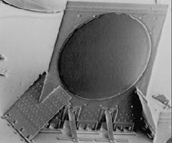
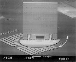
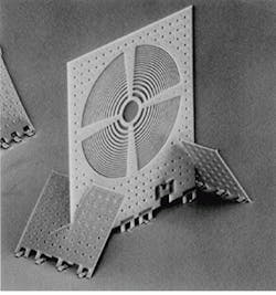
FIGURE 1 (far left). Three-dimensional micro-Fresnel lens fabricated on silicon free-space micro-optical bench has a diameter of 180 ?m, a focal length of 500 ?m, and an optical axis 254 ?m above the silicon surface. Additional lens mounts enhance the mechanical strength and precisely fix the angle of the lens.
FIGURE 2 (center). Out-of-plane spherical microlens fabricated by surface-micromachining processing and photoresist reflow is
300 ?m across and has a 645-?m focal length.
FIGURE 3 (right). Tunable Fabry-Perot filter (less than 400 ?m wide), integrated with a rotation stage for angular fine adjustment, offers a tuning range of 58.5 nm at 1.3 ?m.
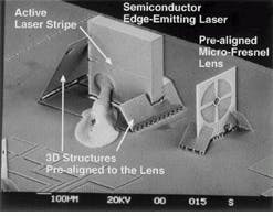
FIGURE 4. Side-mounted semiconductor edge-emitting laser has been hybrid-integrated on the free-space micro-optical bench and prealigned to the focal point of a micro-Fresnel lens.
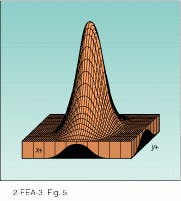
FIGURE 5. Collimated beam profile from the integrated laser/micro-Fresnel module shows well-behaved Gaussian beam. The profile asymmetry is characteristic of edge-emitting diode lasers.
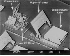
FIGURE 6. Monolithic beam-steering device integrated with an upright-mounted semiconductor laser changes the beam optical-axis height from 120 ?m (thickness of laser substrate) to the free-space micro-optical bench standard of 254 ?m.
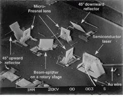
FIGURE 7. Free-space micro-optical disk pickup head consists of a prealigned semiconductor laser, a collimating lens, a beamsplitter, a focusing lens, a 45! upward-reflecting mirror and a 45! downward-reflecting mirror. The reflected signal is collected by the focusing lens and directed by the beamsplitter and the downward mirror to a photodetector integrated on a silicon substrate.