INTEGRATED OPTICS: Deformable mirror tunes VCSEL over 15 nm
A 0.5-µm-thick membrane fabricated over a vertical-cavity surface-emitting laser (VCSEL) creates an external cavity whose length can be varied, thereby allowing the device output to be tuned over a range of 15 nm. Electrostatic force from an applied voltage varies the thickness of the air gap between the semiconductor cavity and the membrane. The device de monstrated a minimum threshold current of 35 mA for the 15- to 23-V tuning bias range investigated, operating in pulsed mode at room temperature. Device center wavelength, l0, was 960 nm, and an output power up to 230 µW was obtained.
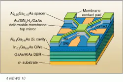
Aluminum gallium arsenide spacers support the membrane above the VCSEL, creating an air gap nominally 720 nm thick (see figure). The membrane itself consists of a 67-nm-thick layer of GaAs overlaid by a 380-nm-thick silicon nitride (SiNxHy) layer, topped by a gold film. The central reflector is approximately 16 µm in diameter. The three layers are present both to achieve high reflectivity and to eliminate mechanical bending from nonuniform thin-film stress.
In conjunction with the air/semiconductor-cavity interface, the air gap and membrane effectively form a distributed top-cavity mirror that imposes a tunable phase shift on the VCSEL output. This phase shift varies the resonant wavelength of the device, and light is coupled out of the device through the n+ substrate.
The bottom cavity mirror is a 22.5-period, n-doped gallium arsenide/ aluminum arsenide (GaAs/AlAs) distributed Bragg reflector (DBR). An Al0.4Ga0.6As cavity spacer containing three 5-nm In0.2Ga0.8As/GaAs quantum wells within a PIN diode, overlaid with a half-wavelength p-doped GaAs current-spreading layer completes the 580-nm cavity. Four p+ metal contacts overlap the edge of the semiconductor cavity; proton implantation defined the electrically active region of the device.
Device fabrication and performance
A group of Stanford University (Stanford, CA) researchers led by Michael Larson fabricated the DBR, cavity spacer, and current-spreading layer by molecular-beam epitaxy (MBE). After applying a sacrificial layer of Al0.85Ga0.15As by this same method, they topped it with a 67-nm-thick layer of GaAs. The applied voltage acts only to contract, not expand, the air gap; to provide maximum tunability, Larson designed the sacrificial layer to produce a gap slightly greater than the required 720 nm. The silicon nitride layer was applied by plasma-enhanced chemical-vapor deposition. To offset the intrinsic tensile stress of this layer and eliminate bending, the electron-beam-evaporation-deposited gold film was 120 nm thick.
For applied voltages ranging from 15 to 22.6 V, the researchers obtained output ranging from 967 to 952 nm; the wavelengths were detected at more or less evenly spaced intervals across the range. The device exhibited nearly resolution-limited linewidths of 0.14 nm. Larson attributes the low output power of the laser primarily to loss in the top mirror, as well as leakage current and quantum-well design.
About the Author
Kristin Lewotsky
Associate Editor (1994-1997)
Kristin Lewotsky was an associate editor for Laser Focus World from December 1994 through November 1997.