Tapping-probe phase imaging increases atomic force microscope contrast
Tapping-probe phase imaging increases atomic force microscope contrast
John Thornton
In conventional atomic force microscopy (AFM), a fine-tipped probe mounted on a flexible cantilever scans across the surface of a sample. By monitoring cantilever deflection resulting from sample topography, the microscope generates images of the surface under test. This technique, called contact-mode AFM, has some drawbacks, however; probe-to-sample normal force can damage samples, and lateral force applied during the scan can deform or tear fragile surfaces.
TappingMode AFM, developed by Digital Instruments (Santa Barbara, CA), provides nanometer-scale information about surface structure while avoiding difficulties experienced with the conventional approach. The system acquires topographical information nondestructively in three dimensions, with a horizontal resolution of 1 to 5 nm and a vertical resolution of 0.5 Å. Phase imaging, an extension of tapping-mode AFM, simultaneously detects variations in adhesion, viscoelasticity, and composition of materials. Applications of phase imaging include identification of contaminants, component mapping in composite materials, and differentiation of regions of high and low surface adhesion or hardness.
Tapping-mode microscopy
In TappingMode operation, a piezoelectric driver excites a single-crystal silicon cantilever/probe assembly into a resonant oscillation; the probe then lightly "taps" on the sample under test. Contact with the sample modulates probe motion, yielding a variety of characteristics about the sample.
When not in contact with a sample, the cantilever typically oscillates at 300 kHz with a peak-to-peak amplitude of approximately 60 nm; contact with the sample damps this value by 5% to 10%. An optical probe motion-monitoring system tracks the amplitude change as the probe moves relative to the sample, and a feedback loop adjusts the vertical displacement of the scanner to maintain a constant oscillation amplitude. The average vertical displacement of the scanner at each data point is used to form the topographical image of the surface.
Compared with contact AFM, the TappingMode approach applies very low normal force and virtually eliminates probe-to-sample lateral force, while still offering the high resolution of a contacting technique. These factors make it possible to image soft, fragile, and adhesive materials without the risk of sample damage.
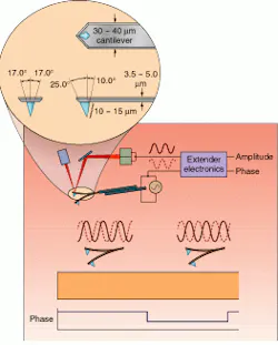
Cantilever motion, the critical element of the system, is monitored by an optical lever, or beam-deflection system. A 1-mW diode laser operating at 670 nm illuminates the back of the cantilever. The resultant reflected beam travels to a turning mirror, which relays the beam to a split-diode photodetector (see Fig. 1). As the cantilever moves from vertical minimum to vertical maximum, the reflected beam illuminates the lower, then upper, segments of the photodiode. The rms value of the electrical signal representing the optical oscillation is sent to the feedback loop. De pending on the system, the probe moves relative to a stationary sample or the sample moves relative to a stationary probe.
Phase-imaging mode
In phase-imaging mode, the system records the phase shift of the cantilever oscillation with respect to the excitation signal sent to the cantilever piezoelectric driver. A cantilever driven at its resonance frequency has a phase lag of 90° relative to the drive. Various interactions between the tip and sample (adhesion and compliance) can shift the phase lag relative to the resonance value. The phase image is formed by mapping this phase shift at every x,y data point.
The resolution of phase imaging is comparable to the resolution of topographical mode imaging. It provides more information about the sample while requiring no additional effort from the user. Phase imaging can act as a real-time contrast-enhancement technique. Because the method highlights edges and is not affected by large-scale height differences, it permits clearer observation of fine features, such as grain edges, which can be obscured by rough topography.
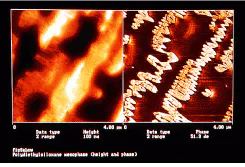
Phase imaging can detect surface contaminants and evaluate processing steps in integrated-circuit manufacture. The technique can determine the distribution of materials in composites or variations in material states. The amorphous and partially ordered states of polydiethylsiloxane demonstrate varying degrees of birefringence when imaged optically. The difference between the two materials, clearly visible in phase imaging, is not apparent in the topographical scan (see Fig. 2). The bright contrast in the phase image indicates 80- to 120-nm-wide lamellar structures of the partially crystallized material state--features that cannot be distinguished with conventional optical techniques.
The contrast in the image appears to result from the variation in stiffness between the two material states; however, other probe-sample interactions may also affect the phase signal. Although there is currently no simple correlation between phase contrast and a single material property, phase imaging can potentially provide useful information for a wide range of applications, in some cases giving contrast where none was anticipated from the material properties. o
FIGURE 1. Output from a diode laser reflects from the back of a vertically oscillating cantilever (inset), propagating to a split photo diode by way of a turning mirror. As the cantilever moves from vertical minimum to max imum, the beam reaches the bottom and then the top half of the photodiode. Contact with the sample surface modulates the oscillation from an undisturbed reference signal; amplitude- and phase-modulation data yield sample information. The cantilever/probe as sembly is etched from single-crystal silicon.
FIGURE 2. Topographical image of polydiethylsiloxane (PDES) deposited on a silicon substrate (left) captures surface morphology, while phase imaging (right) clearly shows the difference between the amorphous and partially crystallized PDES.


