Holographic elements fanout laser beams
Holographic elements fanout laser beams
Beam routing with polymeric holographic optical interconnects provides flexibility in wavelength-division multiplexing and backplane applications.
Ray T. Chen
Holographic optical elements (HOEs) provide several critical beam-routing features that are not achievable through other means. Recently, both micro- and macroscale applications based on HOEs have been realized. Advancement in photopolymeric material has made the fabrication of both transmission and reflection volume holograms reliable and cost-effective. Optical interconnects are generally a better choice for interconnecting different processors and memories whenever conventional electrical interconnects cannot fulfill system requirements.
Holographic optical elements have become increasingly important for these applications. HOEs outperform other existing photonic devices in manipulating coherent lightwave propagation for one-to-many fanout and many-to-one fanin interconnects, which are two of the most important scenarios in backplane and inter-multichip-module communications.
Wavelength-division multiplexers
A wavelength-division multiplexer (WDM) is considered to be one of the key elements for enhancing the transmission bandwidth of optical communications and sensor systems. During the last 20 years, various types of WDMs and wavelength-division demultiplexers (WDDMs) have been proposed and demonstrated. Recently, the technique for producing spatially multiplexed phase hologram WDMs has been developed.
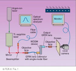
We have built a surface-normal WDM using photopolymer-based volume holograms in conjugation with gradient-index (GRIN) rod lenses.1 In the initial demonstration, multiple-wavelength beams were provided by a Ti:sapphire laser that will be replaced by a diode-laser array (see Fig. 1). The elimination of edge-coupling significantly enhances the packaging reliability.
In the experimental setup, two photopolymer-based volume holograms were used. The collimated light from the single-mode fiber was diffracted by the input hologram coupler and then zigzagged inside the waveguiding plate. It was subsequently coupled out by the output hologram. The output GRIN rod lens focused light beams with different incident angles to discrete spots corresponding to different wavelengths. A charge-coupled-device camera took the pictures. Parameters such as spot size, channel separation, and crosstalk were measured.
In our experiment, the average channel separation was 80 µm, and the average spot size was less than 60 µm, which can be theoretically reduced to less than 5 µm. Current spot size is well above the theoretical prediction due to the implementation of 1/4-pitch GRIN lens. The average crosstalk was less than -20 dB.
Optical backplanes
To increase the interconnection capacity, optical solutions have been considered, but until recently, the burden of electrical-to-optical and optical-to-electrical conversions has prevented the use of optical solutions. Development of efficient optoelectronic devices, especially in the form of arrays, has stimulated research seeking feasible optical solutions, although no general optical backplane compatible with existing electrical buses has been developed yet.
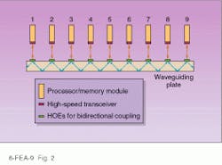
To provide a competitive optical solution, we developed a bidirectional optical backplane with nine processor/memory boards. Unlike the previous optical backplanes aimed at special-purpose computers, the backplane we used is general purpose and thus is compatible with standard multiprocessor backplane buses such as Futurebus+ and Multibus II, as well as any existing backplane bus (see Fig. 2) The backplane bus must provide a path for the bidirectional signal flow among the nine boards. To meet this goal, we used an array of multiplexed holograms in conjunction with a waveguiding plate. An electrical transceiver at each processor/memory board drives the corresponding diode laser located at the bottom of the board. The light from the laser is then bidirectionally coupled through a multiplexed hologram into the substrate, which acts as a waveguiding plate. The surface-normal fanouts are provided by an array of holograms located between the backplane and the processor/memory boards. The photodiode associated with each signal line detects light coming from either direction in the waveguiding plate.
The signal is coupled into the backplane through a hologram acting as an input coupler, which is designed to provide a total-internal-reflected beam within the waveguiding plate. An array of multiplexed holograms is recorded along each signal path.
Grating vectors corresponding to the two gratings are recorded inside the polymer film. A normally incident light is phase-matched with the gratings, both of which have the same Bragg angle. As a result, two diffracted beams will be generated by the hologram and converted into substrate-guided waves in two opposite directions. During the subsequent waveguiding processes, when the substrate-guided beam hits the multiplexed hologram with a Bragg angle, it gets diffracted, generating light necessary for the bidirectional optical backplane. The light diffracted surface-normally out of the backplane is detected by the photodiode. The optimization of the diffraction efficiencies associated with each multiplexed hologram is needed to minimize the dynamic range of the power received at each board.2
Each multiplexed hologram acts as an input coupler to split a surface-normal TEM00 laser beam into two substrate-guided beams with a predesigned bouncing angle of 45°. The same hologram couples a substrate-guided beam into a surface-normal fanout beam with a specific coupling efficiency. For example, the multiplexed hologram at board 5 in Fig. 2 couples the optical signal from itself to boards 4, 3, 2, and 1 through one grating and to boards 6, 7, 8, and 9 through the other grating. These two gratings are physically multiplexed on top of the waveguiding plate. The same hologram will couple signals generated from boards 4, 3, 2, and 1 to board 5 through the first grating and from boards 6, 7, 8, and 9 to board 5 through the second grating.
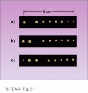
The dots in Fig. 3 represent the input beams going to the detectors located on each board. Azimuthal symmetry of the profile is maintained,3 which makes the coupling from the laser to the backplane and then from the backplane to the detector relatively easy. Unlike conventional guided-wave devices, where a sizable portion of the surface area is needed to provide the optical signal routing, the substrate-guided-wave-based interboard interconnect does not require any surface area for this purpose. The main advantage of our optical backplane stems from its ability to provide the cascaded fanouts with a signal flow in both directions.
A 1.2-Gbit/s signal is fed to the transmitter. The input is a differential ECL signal and is obtained from a high-speed pulse generator. A high-speed sampling head is used in conjunction with an oscilloscope to display the output.
The optical backplane consists of multiplexed holograms in conjunction with a waveguiding plate with cascaded fanout capability. A bidirectional optical backplane with nine boards has been demonstrated. A data-transfer rate of 1.2 Gbit/s at 1300 nm was shown with a single bus line. The bidirectional optical backplane is transparent to all the higher layers of electrical bus protocol and can support all kinds of buses, including high-performance multiprocessor buses, as long as the appropriate protocols governing the rules of data transaction are provided. All the existing protocols for electrical buses can still be used for the optical backplane.
We also fabricated a new hybrid optical backplane with multiple bus lines. It is based on the same waveguiding structure, but the overall scheme for the integration with the electrical environment will be different. It utilizes an optoelectronic array device, the size of which determines the number of bus lines on the backplane.
HOE-based delay lines
Phased-array antennae (PAA) offer many advantages, including steering without physical movement, accurate beam pointing, increased scan flexibility, precise elemental phase and amplitude control to obtain low spatial side lobes, and reduced power consumption and weight. PAA systems combine the signals from as many as several thousand antenna elements to point a directive beam at some angle in space. The characteristics and angle of the beam are selected electronically across the array elements using analog or digital control of the amplitude and phase of excitation. Such an electronic phase control is accomplished through bulky, heavy coaxial waveguide feed. Furthermore, as higher-frequency phased-array operation is pursued, element spacing will become increasingly tight, making waveguide congestion and crosstalk at the array backplane serious concerns.
Most of these control functions can be performed by photonic systems. For instance, photonic systems can be used to provide true-time-delay transmission paths for the microwave signals that are distributed to array elements.
The wide bandwidth promised by true-time delay is due to a fixed set of delay lines that compensate for the path differences corresponding to a particular steering angle qo over an ultralarge microwave bandwidth. Steering of the angle is achieved by turning on and off each detector independently.4 The more delay lines, the more angular selections are provided. The spatial multiplexibility and demultiplexibility of the proposed idea generates more delay lines per area, and therefore a more accurate angle selection system is provided.
Although broadband potential has long been recognized, the true-time-delay approach is not commonly implemented in electronics because it requires the use of heavy, bulky coaxial cable/waveguides serving as RF delay lines. Spatially multiplexed HOEs offer a lightweight, compact solution to highly accurate true-time-delay steering of microwave phased-array antennae.
The bandwidth and delay time product of fiberoptic delay lines is limited only by the optical dispersion of the waveguiding plate. The proposed optical delay line is eventually nondispersive over the frequency range of interest due to the small tuning range of the optical wavelength (1 nm is equivalent to ~300 GHz ).
Optical fanout of various delay lines is accomplished by HOEs. These HOEs couple the light into and out of substrate modes from the surface-normal directions. By selecting the proper thickness for a holographic film with a given index modulation, close to 100% diffraction efficiency has been realized for a desired reconstruction wavelength. Further increase in film thickness results in lower diffraction efficiency, a condition referred to as overmodulation. Diffraction efficiency can be controlled by varying the photoexposure dosage or the ratio of the two interference beams. To achieve such fine tuning on the diffraction efficiency, a thorough understanding of the photopolymer-film characteristics is necessary.
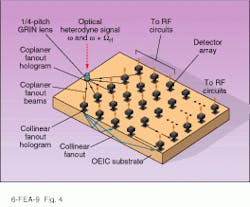
Uniform fanout intensity is required for a practical system. To ensure that the fanout optical signals from each output coupler are uniform in intensity, it is necessary to fine-tune the diffraction efficiency from each output coupler. With the coherent mixing of two CW lasers oscillating at single longitudinal frequencies, microwave signals can be generated by optical heterodyne techniques. The outputs of two tunable diode lasers with a lasing wavelength around 786 nm are combined by a 50:50 beamsplitter, passed through an optical isolator, then coupled into the waveguide by a prism coupler at a suitable angle of incidence (see Fig. 4).
The optical signal is coupled out of the waveguide through another prism coupler and then to a single-mode fiber with a 20X microscope objective lens. The output of the fiber is launched directly to an ultrafast photodetector with 60-GHz bandwidth through the matched FC connector. The photodetector output is amplified through a broadband amplifier and immediately connected to a spectrum analyzer for display. The photocurrent output from the photodetector contains a dc element and an ac element corresponding to the high-frequency RF beat signal. The advantage of this approach is that the modulation depth and the micro wave frequency thus generated are much higher than direct modulation of a diode laser.
We have successfully produced and detected micro wave frequency signals from 1 GHz up to 50 GHz but have been limited by the frequency response of the amplifier and the spectrum analyzer used. Because fine-tuning of the laser wavelength (a few angstroms) will provide a large beat frequency, soon it will be possible to generate wideband RF signals up to 100 GHz. In fact, microwave signals as high as several hundred gigahertz have already been achieved, hindered only by the difficulties of detecting and demonstrating such signals.
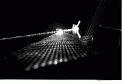
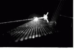
By using external mixers and wideband amplifiers, signals of much higher frequency are expected. Feasibility of manipulating the HOE arrays with an accurate diffraction efficiency is being studied. The photo on p. xxx illustrates a massive fanout containing 30 delay lines using multiplexed holographic grating couplers. For the purpose of demonstration, the display wavelength in this photo is 514 nm. Each fanout beam is provided through the corresponding Bragg diffraction. The total diffraction efficiency is 92%, with power fluctuation within +3% among all 30 fanout beams. n
ACKNOWLEDGMENTS
This research is currently sponsored by AFOSR, ONR, BMDO, the ARPA Center for Optoelectronics Science and Technology, Cray Research, DuPont, Amoco, GE, Radiant Research, and the State of Texas. Thanks to Charles Lee, Yoon-Soo Park, and Bob Leheny for their help and encouragement and to Willie Ng of Hughes Research Laboratories for technical support. Thanks also to the researchers in the Optical Interconnects Research Group at UT Austin.
REFERENCES
1. M. Lee and R. T. Chen, Opt. Lett. 20, 797 (1995).
2. C. Zhao and R. T. Chen, Opt. Engineer. 35, 983 (1996).
3. S. Natarajan, C. Zhao, and R. T. Chen, IEEE J. Lightwave Technology, Special Issue on Optical Interconnects 13, 1031 (1995).
4. R. T. Chen and R. Lee, SPIE Photonics West 2689-25, "Holographic Optical Elements for True-Time-Delays Aimed at Phased Array Antenna Applications" (in press).
Thirty true-time-delay lines are created by 30 fanout beams from multiplexed holographic grading couplers.
FIGURE 1. Configuration for experimental setup measures the wavelength-division demultiplexer (WDDM) channel separation. The system architecture is compatible with the implementation of vertical-cavity surface-emitting lasers where surface-normal coupling is required. Azimuthal symmetry is maintained in the waveguiding substrate when a TEM00 beam is used.
FIGURE 2. Optical bidirectional backplane bus in a multiprocessor system has nine processor/memory modules and nine bidirectional HOEs.
FIGURE 3. Second(a), third(b), and fourth (c) boards send optical signal to the other boards through the bidirectional optical backplane.
FIGURE 4. Setu¥shows the generation of microwave signals by optical heterodyne detection.
RAY T. CHEN is a professor at the Microelectronics Research Center, J. J. Pickle Research Campus, University of Texas, Austin, TX 78758; email: [email protected].
