Prisms march in array for optical interconnects
Free-space optical interconnects-intended for communication between integrated-circuit chips-typically contain two-dimensional arrays of active elements such as detectors and vertical-cavity surface-emitting lasers (VCSELs), with more-tightly packed arrays capable of higher data-transmission rates. Such interconnects often require the placement of micro-optical components such as lenses or prisms in front of each active array element. Arrays consisting of lithographically fabricated binary diffractive optics can be constructed to precise tolerances for this purpose. Because of the resolution limit of the lithographic process, however, as the size of individual optical elements is made smaller, the number of binary phase steps decreases. The result is reduced diffraction efficiency.
Researchers at the Optische Nachrichtentechnik (ONT), Fernuni versit?t Hagen (Hagen, Germany), and the Institut f?r Angewandte Physik, Friedrich-Schiller-Universit?t Jena (Jena, Germany), have created a practical alternative to the use of diffractive micro-optical prism arrays that retains high efficiency even when its individual prisms are very small. Their technique relies on a fabrication method called analog lithography, which is based on photomasks that have gray-level capability.
Such a photomask is made of high-energy-beam-sensitive glass containing silver-alkali-complex halide crystals, which darken upon exposure to an electron beam (e-beam). Direct writing of the glass with an e-beam creates the mask`s gray scale, with the beam variable being dwell time, current, or acceleration voltage. The glass is doped with an ultraviolet (UV) photoinhibitor so that subsequent use of the mask with UV light for lithography does not darken it further. The optical density of any point on the mask can be made anywhere from zero to 2.6.
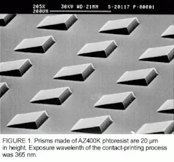
Combined with standard lithographic contact-printing techniques, the gray-scale photomask makes possible the fabrication of variable three-dimensional relief patterns in ordinary photoresist-in this case, microprisms 100 ? 100 ?m square and from 6 to 20 ?m in height (see Fig. 1, on p. 32).
The researchers smooth the prism faces by heating the prism array in an oven, causing the photoresist to reflow slightly. Bake temperature ranges from 70°C to 80°C at durations of 18-24 h, according to Christiane Gimkiewicz, doctoral student at ONT. "The higher the temperature, the better the surface smoothing of the photoresist," she explains, noting that softening and curving of the prism edges places an upper limit on oven temperature.
The researchers then transform the prisms into fused silica by reactive-ion etching. In one example, photoresist prism arrays of 6-?m height were transformed into fused-silica prism arrays of 4.2-?m height. Although the melting and smoothing technique reduced the usable prism area to approximately 82 ? 82 ?m, the result was a transmission that reached 95% of ideal. Optical testing confirmed the importance of resist reflow to surface smoothness of the final glass surfaces (see Fig. 2).
The prisms can be fabricated either in fused silica or gallium arsenide (GaAs), according to the researchers. In use, a prism array of fused silica would consist of a separate unit placed close to a VCSEL array. If made from GaAs, the prism array would be formed on the VCSEL substrate itself, with the emitted VCSEL light passing through the substrate and exiting via the prisms. With a refractive index of 3.63, GaAs would allow deflection angles of up to 40° for shallow etch depths.
The researchers are concentrating on increasing the etch rate between fused silica and photoresist, says Gimkiewicz. This increase will translate into greater prism height. "We have realized smooth glass prisms with heights up to 15 ?m," she adds.


