Micro-optical integration spurs mass production
Micro-optical integration spurs mass production
Combining diffractive and refractive optical elements with lasers and photodetectors creates miniature integrated optical systems.
Adam Erlich
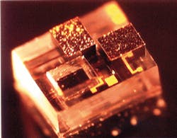
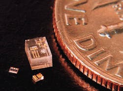
The development of integrated micro-optical systems (IMOS) represents a significant advance for optoelectronics, and IMOS could be considered the optical equivalent of the integrated circuit. Whereas integrated-circuit technology makes it possible to shrink large systems of transistors into a much smaller element, the IMOS process converts a large and expensive macroscopic optical system into a microscopic optical system. Digital Optics Corp. (DOC; Charlotte, NC) has been able to create IMOS systems that include lasers, electronics, refractive and diffractive lenses, and photodetectors on a 2 ¥ 2 ¥ 2-mm cube (see Fig. 1). Currently, several manufacturers are using IMOS technology to reduce the size and cost of their systems.
The diffractive and refractive optics are fabricated using techniques that are similar to those used to make micro-chips. We have utilized that core manufacturing technology to miniaturize an entire optical system including refractive and diffractive optical elements, lasers, and electronics. All of these components are either fabricated or bonded on the same substrate with micron and submicron accuracy. Rather than dealing with macroscopic optics and actively aligning them, entire microscopic optical systems, including lasers and electronics, are fabricated or die-bonded at the wafer level. This fabrication is done with such a high degree of precision that it makes active alignment unnecessary.
Optically tracked floppy disk drives
DOC`s expertise as a diffractive optics manufacturer attracted a company that had designed an optically tracked, magnetic floppy drive. Because the drive uses an optical tracking system, the drive company needed an element that would have required many conventional lenses. With diffractive optics, however, a single 5 ¥ 5-mm element composed of different diffractive lenses and gratings was designed and fabricated. Soon after the element was prototyped, it was mass-produced in glass.
The diffractive element was attached to an optical head
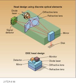
1.5 in. long and 1 in. wide. The optical system included the diffractive element, macroscopic refractive lenses, and a mirror block. The optical head also included a diode laser and photodetectors (see Fig. 2). The diode laser in a conventional can is positioned in a mount so as to direct the light from the laser toward a conventional plastic refractive lens. The refractive lens focuses the light onto the storage media. In addition, a diffractive element is used to split the light to create multiple overlapping spots on the media in precise locations that correspond to optical marks placed on the disk media. The reflected light is then imaged by a second refractive plastic lens onto a photodetector. The signals received by the photodetector are used to obtain tracking information needed to align the magnetic head. The alignment of the components is tight, requiring a tolerance limit of approximately 30 µm to ensure proper location of the signal spots on the media and on the detector.
Miniature laptop elements
Soon after the completion of the prototype desktop disk drive, the development of the next-generation drive for laptop computers was initiated. For this project a much smaller optical head was required. To fit in a slimline laptop, the optical head needed to be reduced by approximately a factor of 10 in each dimension, which corresponds to a factor of 1000 in volume. The principal problem in shrinking the head to these dimensions was to find a way to do this economically while maintaining the required alignment tolerances. In general, the alignment tolerances of optical systems scale with dimension. In this case a 10X reduction resulted in an alignment tolerance requirement of less than
3 µm.
Traditionally, elements with complex optical systems are either actively aligned or parts are machined to tight tolerances in order to avoid active alignment. Actively aligning parts is relatively expensive, while machining to tight tolerances is insufficient to meet the needs of many optical systems. In telecommunications applications, electronic packaging methods have been used to create relatively simple electro-optical elements that are coupled to a fiber with micron accuracy and are made in high volume. The IMOS process uses electronic packaging techniques in combination with photolithography to make multilens microscopic electro-optical elements, which provide the same or better accuracy than active alignment without the high cost. Furthermore, wafer-level photolithographic fabrication makes it possible to fabricate very small elements that can be reliably mass-produced.
The first challenge in applying the IMOS technology to this program was to develop a method to assemble diffractive and refractive components with extreme accuracy, but low cost. This was accomplished by bonding a wafer of diffractive elements to a wafer of refractive elements. By bonding together entire wafers of elements, the alignment step was accomplished on hundreds of dies simultaneously, which is significantly less expensive than bonding each
element one at a time. The lateral alignment of better than ۬ µm was accomplished by modifying photolithography equipment. The spacing between the refractive and diffractive lenses was achieved through precision etching of the glass wafers to achieve precise mechanical spacing elements.
The actual bonding of the monitor detector, diode laser, and signal detector was accomplished after the wafer bonding with the aid of metal solder pads and alignment marks. These marks were fabricated directly onto the fused silica substrate, allowing the electronics to become an integral part of the package. Accurate placement of the solder pads is achieved by precision "through wafer alignment." Placement of the solder pads on the optical substrate is critical in providing a compact optoelectronic package that includes electronic chips as well as optical components. The precision solder pads facilitate the placement of electronic components with a very high degree of precision in a method compatible with mass production.
The next hurdle that DOC needed to overcome was to convert a prototype into an element that could be mass-produced with high yields. Also, on-site automated profilometry equipment and optical testing stages were used along with statistical process controls to provide constant feedback during the production process. Ultralow particle counts were required in order to prevent contamination of the photoresist. This made it necessary to do portions of the fabrication in a Class 10 clean-room environment. Through carefully monitoring the production process and optimizing both the production environment and the inputs, yields were significantly improved. For production following prototype development, changes have been made to the way the electronics are attached and to the heat sinking of the laser, but the overall size has remained substantially the same. DOC and the disk drive company have teamed with a large electronics company for the production of these elements.
Ramping up production
DOC is currently increasing production of the optics for this optical head product and has near-term plans and the capacity to ramp up to several hundred thousand elements per month. In addition to this project, there is a wide range of additional applications. These include other data-storage products, laser modules, and completely new applications that take advantage of the small size and low cost of the element.
DOC is working with another data-storage company to create an IMOS element that will be used in an optical read head and is also developing generic IMOS elements that can be used as electro-optical building blocks for larger systems. There are many potential applications for lasers and optics that have not been viable because of the high cost of a precision-aligned electro-optical system or large module size. The IMOS process has the potential to catalyze the development of new categories of photonic products.
The optoelectronics industry is experiencing a revolution akin to the one that occurred in the electronics industry when the integrated circuit was invented. Before the integrated circuit, making an electronic system involved painstaking care, hand assembly, and high failure rates. The optics industry has been using similar techniques to make optical systems. The IMOS fabrication process offers the possibility of using semiconductor fabrication techniques to mass-produce high-quality, miniature integrated optical systems that are assembled with micron alignment accuracy. Just as the integrated circuit spawned a multitude of new electronic applications, IMOS offers the same potential for the optoelectronics industry. o
ACKNOWLEDGMENTS
A number of DOC employees contributed to the IMOS project. Vice president Alan Kathman led the effort; Bill Delaney, chief fabrication engineer, did experimentation and fabrication of the elements; and Waddie Hayward, VLSI designer, designed the electronic leads, solder pads, and alignment marks. Additional contributions to this effort came from Bob Te Kolste, vice president of manufacturing, and Hongtao Han, director of optoelectronic packaging.
FIGURE 1. Prototype integrated micro-optical system for an optically tracked floppy disk drive is considerably smaller than a dime.
FIGURE 2. Novel design for an optical head shrinks complex optical system from 1.5 ¥ 1 in. (top) to 2 ¥ 2 mm (bottom).
ADAM ERLICH is sales account manager at Digital Optics Corp., 5900 Northwoods Parkway, Ste. J, Charlotte, NC 28269.


