AFM helps engineer low-scatter thin films
AFM helps engineer low-scatter thin films
Angela Duparr and Norbert Kaiser
Proper use of power-spectral-density
measurements
made with an atomic force microscope
can help optimize thin-film coatings
for low scatter.
The quality of optical components used in complex applications such as lasers, microscopes, and lithography systems is critically influenced by their surface morphology. The majority of these components?including lenses, mirrors, beamsplitters, and polarizers, for example?are covered by thin-film optical coatings. Hence, important properties of the optical elements?particularly optical scattering?are directly related to the surface microstructure of the thin-film coating. Given the ongoing trend of optical lithography toward shorter wavelengths, such as lithographic objectives shifting from 248 to 193 nm, thin-film researchers are facing increasing requirements for low-scatter ultraviolet (UV) optics.1
Surface microstructures of thin films can be measured with an atomic force microscope (AFM), and the results can substantially contribute to successful development of low-scatter optical coatings. This does, however, require a good understanding of some basic relationships between microstructures and optical scatter, as well as the use of appropriate AFM data-analysis and interpretation concepts.
This article discusses aspects of thin-film and substrate surface microstructures as they relate to scatter losses. It does not, however, discuss the purely optical effect of a coating?that is, scattering enhancement due to enhancement of reflection. A thin-film coating that increases reflection also generally will increase scattering when compared to the pure substrate, independent of the film structure, even if the film is totally smooth.2
Power-spectral-density measurements
Fluorides play a key role in UV coatings because of their low absorption at these wavelengths, which is particularly important below 200 nm. All the general principles demonstrated by fluoride-based coatings are valid for other coating materials as well. The AFM measurements described here were performed with a Dimension 3000 AFM (Digital Instruments; Santa Barbara, CA) operating with Digital Instruments TappingMode imaging technique that prevents damage to the thin films and provides optimal image and data quality.
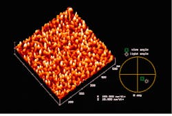
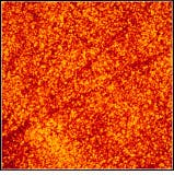
The surface morphology of a 50-nm-thick lanthanum fluoride (LaF3) film on a quartz substrate shows surface features that result from the columnar structure and is typical for many dielectric thin films (see Fig. 1). The image may lead to the assumption that the pronounced structure gives rise to scatter losses. Additional consideration of the increase in rms roughness (with a 500 500-nm scan) from 0.4 nm for the uncoated quartz surface to 1.3 nm after coating would support this assumption. Scattering theory tells us, however, that the amount of optical scatter depends not only on the roughness height of a structure, but also on its lateral distribution.
Any randomly rough surface can be considered as a Fourier series of sinusoidal waves with different amplitudes, periods, and phases. The grating equation shows that a single grating with spacing d causes scatter into the angle Q according to
sin Q = lld
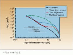
where l is the wavelength of light and d can be considered as one spatial wavelength present on the surface (or f = l/d is one spatial frequency). At a randomly rough surface, such as the thin-film component, many different spatial frequencies are present. This is expressed quantitatively by the power spectral density (PSD), which gives the relative strength of each roughness component of a surface microstructure as a function of spatial frequency.3
To cover an extended range of spatial frequencies, we combined the PSD curves from 1 1- and 10 10-?m scans (see Fig. 2, red curve). One can see that at low spatial frequencies?that is, roughness components of larger lateral extension?the PSD of the coating coincides with the PSD of the substrate (black curve), which means that the substrate microstructures replicated by the film determine the PSD in this region. The thin-film structure is represented by the ObumpO in
the PSD at frequencies greater than 10 ?m?1.
Figure 2 also indicates the spatial-frequency region to which a typical total integrated backscattering measurement would be sensitive when performed in the visible and ultraviolet region.3 The thin-film structure does not cause any measurable scatter at visible or UV wavelengths so the scattering is dominated by the substrate. Hence, the PSD reveals that, in this case, reduction of scatter loss can only be achieved by improving the substrate polish, not by changing the deposition parameters.
The blue curve in Fig. 2 is the PSD for a three-layer system of alternating lanthanum fluoride/magnesium fluoride (LaF3/MgF2) layers on a quartz substrate. Note the overall increase in roughness?to 2.7 nm?relative to the single layer (1.3 nm). The most important change, though, is the shift of the bump toward lower spatial frequencies. In the visible range, this does not cause any major scattering effect, but in the UV the effect is significant.
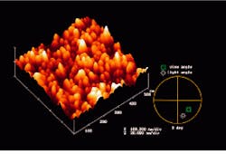
Next, consider a multilayer system consisting of 42 alternating MgF2/LaF3 layers, designed as a high-reflector mirror for 248 nm, again on a quartz substrate (see Fig. 3). The structures have extended both in height and width, with an rms roughness of 6 nm (for the
500-nm scan size). In addition, the PSD (green curve in Fig. 2) reveals that the bump has broadened significantly and extended to low frequencies, indicating that the film structure is now dominating the scatter, even in the visible range.
Scattering measurements
The total backscattering of the multilayer system described was 1% at 248 nm, measured with a total integrated scattering apparatus.4 The scattering of the uncoated quartz substrate was 0.004%. The increase in scattering, attributed to the enhancement of reflection caused by the mirror system, would result in a scatter value about one order of magnitude lower. Thus, the measured scattering of the fluoride coating is actually governed by the microstructure of the films.
This does not mean, though, that in the case of a multilayer system the film structures will be the dominant factor determining scatter, whatever the substrate and the film material. The same fluoride multilayer system discussed was also deposited onto a MgF2 substrate, which is useful in certain excimer-laser applications. Examining 10
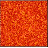
10-?m images of the multilayer system on quartz and MgF2 shows differences, scratches on the MgF2 substrate, that are replicated by the film, but that would not be expected to cause tremendous differences in scattering (see Fig. 4).
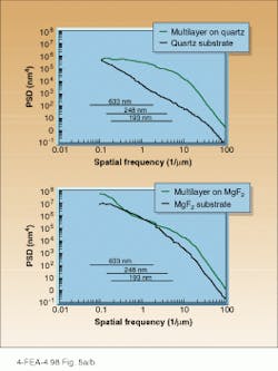
Again, the corresponding PSDs provide the answer. Figure 5 compares the PSDs of the multilayer coating on quartz and MgF2 substrates, respectively. For the coating on MgF2, the PSD indicates that at 633 nm the substrate-related scatter will clearly dominate. The small enhancement after coating around 0.1 to 0.2 ?m?1 is caused by formation of larger defects that occur occasionally when the films are deposited on MgF2 substrates. Even at 248 nm, the influence of the substrate is still significant, and only at shorter wavelengths does the film structure become dominant for the scatter.
This has been shown experimentally. The measured total scattering at 248 nm was 1% for the system on quartz and 3% for the same system on MgF2. So the scatter losses of the two samples differ by a factor of three as a result of the different substrate qualities.
What the PSDs reveal here is that for the system on the MgF2 substrate, any improvement of the deposition process would hardly be worthwhile. This substrate topography effect illustrates the influence substrate polish can have on the overall coating microtopography and related scatter in general. With CaF2, for example, becoming a material of choice in UV lithography, the question of how much polishing quality matters relative to thin-film microstructure is becoming increasingly important?especially because high-quality polishing of this material is difficult to achieve.
In the case of the multilayer system on the smooth quartz substrate, the height and location of the bump in the PSD curve quantify the effect the film structure has on the scattering loss at a particular wavelength. Improvement of the optical coating here requires improvement of the deposition process such that the bump height is reduced (smoother structure) or shifted further out of the spatial-frequency region of scattering (growth of structures with lower diameters). Optimally, both improvements should be achieved.
Predicting scatter losses
Power-spectral-density curves generated with TappingMode AFM data are a valuable and easy-to-handle tool for quantifying the surface microstructure of optical components and for predicting their influence on scatter losses. This is particularly important for thin-film optical components, for which both the substrate and the film structure can give rise to scatter.
Once a thin-film engineer has become experienced in interpreting PSDs, he or she can easily determine whether? for the particular film, substrate, and wavelength of application (that is, where light scatter should be reduced)?the substrate or the film structure or both are the cause of scatter. This helps decide which of the processes, substrate polish or film deposition, has to be improved first.
If the film microstructure is the dominant factor for scattering, the deposition process must be optimized with respect to film structure. This can be efficiently controlled by means of the PSD?adjusting the bump toward the region that is out of the Oscatter barsO?by changing the deposition parameters.
Proper AFM data analysis substantially supports predictions about scatter losses in thin-film optical coatings and, hence, helps reduce these losses through PSD-controlled optimization of the processes. Of course, this does not replace the necessity of direct measurement of the scattering losses of the optical components. In fact, combining the PSD method with two-dimensional total scatter-loss measurements covering the whole area of the component will result in comprehensive knowledge of the microstructure/scatter loss mechanisms and will improve the ability to effectively engineer low-scatter optics. o
REFERENCES
1. N. Kaiser et al., Proc. SPIE 3051, 940 (1997).
2. A. Duparr?, OLight scattering of thin dielectric films,O Thin films for optical coatings, R. Hummel and K. Guenther, eds., CRC Press, Boca Raton, FL, p. 273 (1995).
3. J. M. Bennett and L. Mattsson, Introduction to surface roughness and scattering, Optical Society of America, Washington, DC (1993).
4. A. Duparr? and S. Gliech, Proc. SPIE 3141, 57 (1997).
FIGURE 1. Atomic force micrograph shows surface morphology of a 50-nm-thick
lanthanum fluoride (LaF3) film on a quartz substrate. The surface features that result from the columnar structure are typical for many dielectric thin films.
FIGURE 2. Power spectral density (PSD) is a quantitative expression of the many different spatial frequencies present at a randomly rough surface and is shown here for four different systems. The PSD gives the relative strength of each roughness component of a surface microstructure as a function of spatial frequency. The horizontal lines indicate the spatial frequency region to which a typical total integrated backscattering measurement?with the scattering angle typically extending from 2! to 85!?would be sensitive when performed in the visible and ultraviolet region?in this case at 633, 248, and 193 nm.
FIGURE 3. Morphology of a multilayer system consisting of 42 alternating MgF2/LaF3 layers on a quartz substrate shows that the structures have extended both in height and width. The PSD is shown by the green curve in Fig. 2.
FIGURE 4. Atomic force microscope images
(10 10 ?m) of the MgF2/LaF3 multilayer system on quartz (top) and MgF2 (bottom) substrates show differences?scratches on the MgF2
substrate?that are replicated by the film and cause significant differences in scattering.
FIGURE 5. Power-spectral-density curves of the MgF2/LaF3 multilayer
system on quart¥(top) and MgF2 (bottom) substrates indicate that for the MgF2 substrate at 633 nm the substrate-related scatter will clearly dominate, and even at 248 nm the substrate-related scatter will be significant.
