Nanometrology: NIST scatterfield imaging 'sees' nanometer-scale features
As the size of semiconductor wafer features continues to shrink to low-double-digit nanometer values, inspection equipment is needed to ensure zero defects at reasonable process speeds. Unfortunately, optical microscopes cannot see features much smaller than the wavelength of light used to measure those features and super-resolution microscopy is too slow to meet the inspection speeds required for semiconductor wafers. As a result, scientists are turning to novel inspection techniques such as plasmon rulers and terahertz scanning.
Joining these latter nanometrology tools is a technique from the National Institute of Standards and Technology (NIST; Gaithersburg, MD) that combines standard through-the-lens microscopy with scatterfield imaging.1 By understanding the full three-dimensional (3D) scattered light field from a patterned surface, the method is able to "see" 16 nm features—30 times smaller than the 450 nm wavelength of light used to measure them—and measure them with an uncertainty of 1 nm.
Reconstructing scattered data
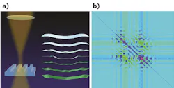
The key to these measurements is to compare simulations of the light scattered off the sample with the actual observations. However, this type of finite target scatters a continuum of frequencies. Furthermore, some of the frequencies captured by the microscope may be attenuated when imaged onto the CCD camera because of imperfections in the system or the design of the physical optics. Once the light is scattered off the sample, there is no way to correct for these losses that introduce error and aberration.
Knowing this, the research team realized it was necessary to correct the electromagnetic simulation outputs for these losses before generating a simulated image. This required a thorough characterization of the microscope—both its illumination optics as well as its collection path. "This scatterfield microscope is equipped with angle-resolved scanning," says Bryan Barnes, physicist and project leader at NIST. "We map out the intensities at the sample as a function of angle, and we repeat the process for the entire optical path by measuring reflected light as a function of transmitted angle using a CCD camera."
Armed with these measurements, the effects of the collection path upon the scattered frequencies are mapped. This map is then applied to the simulated field with its hundreds of spatial-frequency components. This Fourier-domain normalization allows the final simulated images to be compared accurately against the experimental intensity data to find a best fit that yields the width and height, for example, based upon the best-fitting simulation's geometry.
Determining the uncertainties in the measurement requires piecing together even more details about the experiment for a more accurate result. Not only must sources of uncertainty such as repetition be considered, but also estimated uncertainties such as possible shifts in focus or alignment, for example. The results form a specific matrix that directly yields the uncertainties, accounting for otherwise hidden correlations in the measured data.
The researchers intend to extend the technique to measurements with ultraviolet light at 193 nm, allowing accurate measurement of features as small as 5 nm. "It is important to utilize all the information available about these nanostructures," says Richard Silver, physicist and group leader at NIST. "This is extremely useful data when trying to unlock quantitative measurements at the nanoscale. In addition, optics are ideally suited for rapid identification of patterned defects approaching the nanometer scale if one adopts engineered illumination and imaging techniques with shorter-wavelength imaging light."
REFERENCE
1. J. Qin et al., "Deep-subwavelength nanometric image reconstruction using Fourier domain optical normalization," Light Sci. Appl., accepted article preview, e16038 (Nov. 5, 2015).
About the Author

John Wallace
Senior Technical Editor (1998-2022)
John Wallace was with Laser Focus World for nearly 25 years, retiring in late June 2022. He obtained a bachelor's degree in mechanical engineering and physics at Rutgers University and a master's in optical engineering at the University of Rochester. Before becoming an editor, John worked as an engineer at RCA, Exxon, Eastman Kodak, and GCA Corporation.