PHOTOLITHOGRAPHY: Optical immersion further shrinks feature sizes
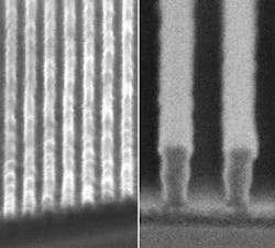
At this year’s annual SPIE Microlithography conference (Feb. 19-24; San Jose, CA), scientists from the IBM Almaden Research Center (San Jose) described results obtained using NEMO, an interferometric tool for deep-UV optical-immersion lithography. They have created distinct and uniformly spaced patterns with ridges and spaces that are only 29.9 nm wide-less than one-third the size of the 90-nm features now in production in the semiconductor industry (see figure). The features are also smaller than the 32-nm size that the industry currently holds as the limit for optical lithography.
The new result indicates that a “high-index-immersion” variant of deep-UV lithography may provide a path for extending Moore’s Law further within the optical realm. Light passing through a higher-index material acts as if it has a shorter wavelength and can be focused more tightly. Resolution in immersion lithography is limited by the lowest refractive index of the final lens, fluid, and photoresist materials. In the NEMO experiments reported at the meeting, the lens and fluid had indices of about 1.6 and the photoresist of about 1.7. Future research is aimed at developing lens, fluid and photoresist materials with indices of refraction of 1.9, which would enable even smaller features to be imaged.
“Our goal is to push optical lithography as far as we can so the industry does not have to move to any expensive alternatives until absolutely necessary,” said Dr. Robert Allen, manager of lithography materials at IBM’s Almaden Research Center. “This result is the strongest evidence to date that the industry may have at least seven years of breathing room before any radical changes in chip-making techniques would be needed.”
Designed and built at IBM Almaden using materials developed by its collaborator, JSR Micro (Sunnyvale, CA), NEMO uses two intersecting laser beams to create light-and-dark interference patterns with spacings closer than can be made with current chip-making apparatus. The system is intended to enable relatively inexpensive researching, testing, and optimizing of the various high-index fluids and photoresists being considered for use in those future DUV systems that would create such fine features (see figure).
“Our industry faces tough questions about which lithography technology will allow us to be successful below 32 nm,” said Mark Slezak, technical manager of JSR Micro. “This new result gives us another data point favoring the continuation of optical-immersion lithography.”
The 2006 SPIE Microlithography meeting broke previous records, with 4250 attendees, up from 4080 last year. Overflow crowds packed numerous technical sessions particularly the plenary and invited sessions, with more than 1150 attendees at the opening plenary session on the morning of Monday, Feb. 20.
Design for manufacturing
The concept of design for manufacturing (DFM) was a recurrent theme, both in technical sessions and on the exhibit floor. In an invited talk on Tuesday morning, Luigi Capodieci, a principal member of the technical staff at Advanced Micro Devices, said that Moore’s Law of exponential growth in circuit density applies not only to density on semiconductor chips but also to the growth of pages in manuals of semiconductor-design rules. There was only one page in 1987. There are 250 pages now, and according to Moore’s Law, there will be 2000 pages upon reaching the 22-nm node, he joked.
As feature sizes on semiconductor chips have gotten smaller than the wavelengths of light with which they are written, the complexity of design rules has grown to ensure that circuits, once manufactured, actually do perform according original design specifications. The complexity of design rules, however, can also lead to designs that are too complex to manufacture at acceptable yields. Design for manufacturing seeks to address such issues by bringing the designer and lithographer communities together in the design process, often assisted by software tools that make the design step more of an iterative modeling and feedback process.
Along these lines, Cymer (San Diego, CA) announced a joint development agreement with KLA-Tencor (San Jose, CA) during the meeting, in which Cymer will provide actual light-source spectral information for incorporation into KLA-Tencor’s lithography software. Synopsys (Mountain View, CA) was also discussing its DFM software roadmap for 2006, which includes new yield-analysis solutions, as well as dual-domain (both space and frequency) simulation capabilities. On the optical-materials side, Corning (Corning, NY) announced the availability of a new high-purity optical-lens material designed specifically to support the performance requirements such as heightened polarization sensitivity of 193-nm immersion-lithography systems.
About the Author
Hassaun A. Jones-Bey
Senior Editor and Freelance Writer
Hassaun A. Jones-Bey was a senior editor and then freelance writer for Laser Focus World.
