CUSTOM OPTICS: New generation of applications raises performance bar for scanning mirrors
Designers must understand the various fabrication trade-offs when specifying custom optics for demanding scanning systems.
DAVID COLLIER AND ROD SCHUSTER
Early galvanometer scanning applications, including barcode scanning and a variety of reprographic tasks, relied primarily on low-power visible or near-infrared lasers. Typically using metal-coated mirrors, these applications weren’t tremendously demanding in terms of optical flatness or surface quality. During the past several years, however, a new generation of more sophisticated scanning systems has emerged to address applications such as micromachining, marking, semiconductor processing, and therapeutic medical procedures. Operating anywhere from the infrared to well into the ultraviolet, and often at high peak powers, these systems require mirrors with high optical performance in terms of reflectivity, wavefront distortion, damage threshold, and lifetime. In addition, mechanical considerations, such as low mirror weight and minimum moment of inertia, are important for these applications.
Scanner background
In a galvanometer scanner, mirror inertia is often the fundamental limitation on the maximum frequency at which scanning can be performed, and on the top acceleration that can be reached. These factors, in turn, can ultimately limit process throughput.
To maximize the mechanical response characteristics of a galvanometer system, then, mirror weight and moment of inertia must be minimized. Typically, this is accomplished by making the mirror as small and thin as possible, and by physically eliminating those parts of the optic that do not actually intercept the beam-leading to the commonly used rectangular optic with “clipped corners” shape. In highly sophisticated systems, it can even result in more exotic, asymmetrical shapes.
Unfortunately, these odd weight-minimizing shapes can drive up mirror costs, particularly when the optic must be tightly specified for other parameters such as flatness or clear aperture. An understanding of how these various factors trade off is critical to obtaining components that meet the scanning system’s mechanical and optical requirements in a cost-effective manner.
Substrate fabrication
Traditional optical fabrication techniques, which use circular motion of round polishing tools, naturally produce a circular clear aperture (defined as the area of the substrate over which the specified parameters apply). For the substrate, the parameter of most concern is usually flatness.
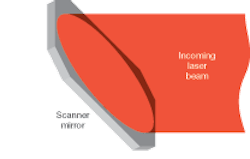
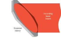
While circular shapes can be easiest to fabricate, a circle of a given diameter possesses less area than a square with sides the same length as the diameter of the circle. Thus, the designer’s first task is to use the beam diameter at the mirror and maximum scan angles to determine exactly what shape and minimum size are required to intercept the beam fully in all cases (see Fig. 1). In order for the mirror to meet its performance specifications at all times, the mirror clear aperture must cover at least the minimum size required for full intercept. As it turns out, the geometry of many scanning applications requires a nearly rectangular clear aperture.
In terms of optical fabrication, producing a round part for which the clear aperture occupies the central 90% of the diameter is relatively straightforward. Similarly, on a rectangular part, an elliptically shaped clear aperture whose major and minor axes are equal in length to 90% of the part length and width, respectively, would yield a conservative specification. Going above 90% of the central area, especially on nonround parts, starts to drive up cost significantly because it requires more polishing time and generally lowers yield. Specifying the clear aperture as extending right up to the part edge represents the extreme case and should be avoided if possible.
What level of flatness is necessary for most scanning applications? Flatness is probably the parameter that is most commonly overspecified by optics buyers because they utilize “industry standard” values, such as λ/8 or λ/10. Flatness ultimately determines minimum focused spot size and should be calculated by the optical engineer to match the specific needs of the application. A flatness specification in excess of λ/10 increases part cost significantly.
Mirror aspect ratio (the substrate diameter or diagonal length, divided by its thickness) also affects the ability to achieve a given flatness specification or clear-aperture value. A thinner substrate minimizes weight and inertia and is most mechanically desirable for scanning purposes. But, once again, this represents the worst scenario for the optics fabricator. Typically, an aspect ratio of 6:1 provides the mechanical characteristics necessary to easily deliver λ/10 flatness parts over a clear aperture of up to 90%. Holding a flatness of λ/8 or better over a clear aperture of more than 85% with an aspect ratio at or greater than 10:1 is considered difficult, and would definitely drive up optics cost. Furthermore, it is difficult to hold tight flatness tolerances on very thin parts (less than 2 mm thickness) no matter what the aspect ratio.
It should also be kept in mind that galvanometer mirrors are used in dynamic situations. Even if a part meets its flatness specification on the test bench, in actual use it can warp out of shape under high acceleration or because of environmental factors like temperature and humidity.
Substrate material is another factor that affects mirror fabrication and in-use performance. There are several materials available for UV, visible, and near-IR wavelengths. Of these, fused silica generally offers better mechanical characteristics, making it easier to achieve a given flatness and to retain it during use.
Coating requirements
Both metallic and dielectric coatings are used widely on galvanometer mirrors. Metallic coatings generally offer lower peak reflectivity, but wider spectral bandwidth, than dielectric thin films. Conversely, dielectric films exhibit higher damage threshold and are typically more mechanically durable and therefore easier to clean.
Although most scanning systems operate at a single wavelength, coating bandwidth is still important because the wavelength of peak reflectivity for dielectric coatings depends on the angle of incidence (see Fig. 2). Variations in angle of incidence of 10° to 20° (around the 45° nominal) are common in scanner systems. These are sufficient to shift the performance of a narrowband coating significantly off its maximum. It is therefore important for the buyer to specify reflectivity, which can be an average or a minimum value, and maximum angular range.
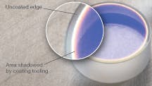
Clear aperture is also a critical specification for coatings because the tooling used to hold a substrate during the coating process typically masks off a few millimeters along the edge of the part. Also, the finite thickness of the coating tooling can create a narrow “shadow,” where layer thicknesses can be compromised (see Fig. 3). Depending upon the shape of the substrate, custom tooling can be created to enable the coated area to reach to at least some of the part edges. This, of course, represents an additional expense. Generally, extending the coating clear aperture to within 1 mm or less of the part edge will significantly increase fabrication cost.
Dielectric coatings can also affect flatness, especially on high-aspect-ratio parts. This is because most dielectric thin films are deposited at high temperature, and mechanical stress is introduced into a coating when the part subsequently cools. The residual stress can be either tensive or compressive and can distort a substrate from its original shape. Unfortunately, the flatness specifications listed by many optics vendors only apply to the substrate prior to coating.
There are various fabrication techniques that can achieve high levels of post-coating flatness. In prefiguring, for example, the substrate is purposefully polished with a slight curvature so that the stress induced by the coating distorts the optic back into flatness. With backside coating a single-layer coating (typically SiO2) is placed on the second surface of the optic in order to offset the overall mechanical stress on the part. It is also possible to create multilayer coating designs in which a combination of materials, having tensive and compressive characteristics, is used to yield an overall film with minimal residual stress.
Assembly considerations
The performance of even the most carefully fabricated optic can be degraded if it is mounted improperly. Stress on an optic is easily introduced during the mounting process and will warp the optic out of its specified flatness. This warping can be caused by mechanical clamping, especially if it is applied asymmetrically, as well as by adhesives that are not applied uniformly or do not cure evenly. Another critical mounting issue is to ensure that the axis of rotation of the mirror is coplanar with its front surface. Dynamic balance of the mirror is also important.
Depending upon the application, it may be desirable to have the optics vendor mount the mirror to guarantee specified performance after mounting. Furthermore, there are handling and mounting issues relating to the cleanliness of the assembly environment and adhesive outgassing that an optics manufacturer is often better prepared to deal with. At the very least, it is useful to have the scanner manufacturer discuss with the mirror fabricator the appropriate mounting techniques and procedures to use to maintain performance of the optic in actual operation.
DAVID COLLIER is president and ROD SCHUSTER is marketing manager at Alpine Research Optics, 6810 Winchester Circle, Boulder, CO 80301; e-mail [email protected]; www.arocorp.com


