OPTOELECTRONICS APPLICATIONS: MICROPROCESSING: ‘Design for manufacturing’ moves farther upstream
For many years the consensus in semiconductor chip manufacturing was that once the feature-writing capabilities of 193 nm optical lithography were exhausted, the next step would be deep-UV 157 nm lithography. And then came Intel’s announcement in 2003 that it was dropping 157 nm tools from its lithography roadmap—a “bombshell” that was followed by a flurry of similar announcements from other chip manufacturers, plus the emergence of liquid immersion as a compelling method for extending the capabilities of 193 nm lithography.
This turn of events put new pressure on the software tools used in the design and production of semiconductor chips. With feature sizes on the chips now smaller than the wavelengths of light used to write them, the complexity of the design rules has grown in concert with the need to ensure that the end product performs according to the original specifications. Among other things, to determine whether a design can be manufactured lithographers must determine how critical features will print across the entire process window.
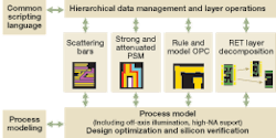
This is where the concept of design for manufacturing (DFM) comes in. As manufacturing and yield issues migrate further upstream into the design process, so does the need to resolve them and produce yieldable products. Generally defined as the tools, flows, people, and expertise necessary to allow a design to enter manufacturing, ramp up quickly, and attain ultimate yield, DFM is not new to chip manufacturing. Corrections have been made between design and manufacturing for more than a decade, and direct optical proximity correction (OPC) has been around at least that long. But with escalating pressure to tackle increasingly complex design, materials, cost, yield, and time-to-market issues, chip designers and lithographers are collaborating earlier than ever before to create a more iterative modeling and feedback relationship throughout the design-to-silicon process, assisted by software tools such as OPC, advanced process control (APC), and reticle enhancement technology (see Fig. 1).
“Lithography ultimately is one of the most critical enablers for continued cost-effective manufacture of semiconductor chips,” said John Sturtevant, technical support manager for resolution enhancement technology products at Mentor Graphics (Wilsonville, OR). “But increasingly everyone is using the same scanners and the same lasers and the same photoresist chemicals from the same small group of vendors. So the ability to differentiate has moved increasingly into the EDA (electronic design automation) space. We can tailor the manipulation of the data in a differentiating and rapid-turnaround fashion, and thus help our customers gain competitive edge by decreasing their time-to market.”
In addition, as feature sizes shrink, so does the process window, which creates an additional set of issues. The smaller the window of settings that will work on any chip, the harder the engineers have to work to ensure they are inside that window. Fortunately, these days the role of DFM is to enlarge the process window with respect to yield, and the role of automated process control is to ensure that engineers stay within that window.
“The process window is getting smaller all the time,” said Ed Charrier, general manager, process analysis division, KLA-Tencor (San Jose, CA). “If you are the engineer trying to manufacture the chip, the production parameters change day to day. You want the chips to work but within a range of possible settings that the equipment is running at on any given day.”
Yield is another core issue behind the broader-scale adoption of DFM. According to Scott Hector, DFM methodology manager at Freescale Semiconductor (Austin, TX), factories have found that for the 90 nm and below, yield is influenced more by systematic errors than random errors. For example, no matter how clean the wafer-manufacturing environment, there are always some small particles in the atmosphere that can land on the surface of the chip. While random errors are difficult to control, it is possible to tweak chip design to minimize their effects on final yield. Systematic errors are essentially manufacturability issues (such as the intensity of the laser and the focus of the lens) that can be identified and addressed in a systematic way—increasingly with the aid of DFM tools.
“The best application of DFM is as early in the design process as possible,” Hector said. “With DFM, a designer doesn’t have to understand all of the physics and chemistry [involved in optical lithography]. If they have a software tool that has codified knowledge of all the processes in the fab, you have a much better solution.”
Model- vs. rule-based tools
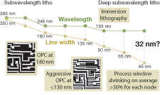
The first DFM tools were rule-based—that is, intended to ensure that the design rules (such as the minimum width of wires or the spacing of redundant vias) for a certain chip were met during the final manufacturing process. But over time, as the features have grown smaller, the number of design rules has grown larger; in the case of the 180 nm node, for example, there were only a few dozen such rules, while the forthcoming 65 nm node is expected to have several thousand. This trend has pushed DFM products to expand beyond standard design-rule and DFM-guideline checking; today, in addition to rule-checking and yield analysis, most DFM products incorporate some combination of chemical, optical, and mechanical modeling and even process simulation (see Fig. 2).“We have to have a very accurate model for the propagation of light through the optical system,” Sturtevant said. “We have to be able to account for a wide variety of optical, chemical, and physical phenomena, so we are continually improving our models to account for all of the possibilities. Our challenge is to deliver very accurate modeling capabilities with very low full-chip run times.”
Mentor’s Calibre products, for instance, have long been used to manipulate design input to ensure that what ends up on the wafer most closely resembles what is on the design. Over time, this rule-based OPC approach has morphed into model-based OPC and even post-OPC verification to account for the optics, error formations, and changes to the photoresist that can occur throughout the litho process and make changes in real time, according to Sturtevant. More recently, Mentor introduced the Litho Friendly Design system, which puts the process modeling capability in the hands of the chip designers to give them the power to make manipulations that will result in higher yields.
At Synopsys, the focus is on offering tools that enable the complete flow of data from manufacturing into design and back again, all with an eye toward improving performance and yield. The company’s DFM focus is on design-rule and compliance checking, place-and-route and extraction tools, technology CAD modeling, and yield management; products range from the Proteus OPC and Hercules design-rule check software to SiVL (silicon vs. layout), a litho-verification tool that considers all process parameters; Sentaurus, which simulates process and device physical behaviors; Raphael for characterizing interconnect structures; and Odyssey, a manufacturing yield-management system.
“If you have the ability at the layout step to invoke a yield analysis system that will essentially take the litho verification system and move it upstream so that hundreds of design rule checks can be done during layout and then run your final litho verification, you end up with a very small number of design problems that you have to deal with,” said J. Tracy Weed, director of manufacturing enabling products for the DFM group at Synopsys.
Similarly, KLA-Tencor’s PROLITH, which was introduced 20 years ago and is considered an industry standard, is a physically based simulator that provides process optimization information, explores the effects of process variables and process performance improvements, and offers a comprehensive representation of the entire optical lithography process. According to Charrier, PROLITH is used primarily by litho engineers and OPC groups to optimize small parts of a design that are problems during manufacturing; by making very accurate simulations of very small areas, PROLITH helps them re-engineer those areas and enlarge the process window. Most recently, KLA-Tencor began collaborating with Cymer (San Diego, CA) to incorporate details of light-source spectra into PROLITH and allow users to model the effects of changes in light source spectral characteristics on their lithography processes, thus optimizing the process and minimizing the effects of any variations. According to Charrier, the effects of laser bandwidth on critical dimensions becomes more significant with higher numerical apertures and shrinking process windows.
Physics and DFM
In fact, the physics behind optical lithography—especially as feature sizes become smaller than the wavelength of light used to create them—is another important driver in the semiconductor industry’s implementation of DFM throughout the design-to-silicon process. In earlier nodes, features and photomasks could be directly replicated on the surface of the silicon chip. But in the 90 nm and smaller nodes, the wavelength of light used to create the patterns on the chip is larger than the structures and wires. The resulting physics creates interference effects that can distort these patterns and photomasks when printed unless detected and accounted for early in the design process.
At the same time, DFM optimization processes have allowed lithographers to push the capabilities of 193 nm lithography further than anyone originally thought possible. In particular, by using DFM techniques in conjunction with numerical aperture (NA) and k1, lithographers have been able to overcome the physics of diffraction-limited optics in the 193 nm realm, achieving a NA of 0.93 and k1 of 0.35. Next up is immersion lithography, which is expected to further extend the NA to 1.3, according to Sturtevant.
“As we go to smaller and smaller dimensions, there have been only three wavelength reductions,” Sturtevant said. “We are looking at using 193 nm for the long foreseeable future. In fact, my personal opinion is that EUV may never see the light of day in full volume production—at least, not like 193 is today. It really comes down to cost of ownership; if the industry looks at wavelength as a knob, we don’t have any immediate cost-effective alternatives. So we look to numerical aperture and k1 instead.”
For some industry experts, however, the real future of optimized collaborative chip design and manufacture lies in TCAD (technology computer-aided design), which involves the use of physics-based statistical modeling to explore new technologies and novel devices, optimize process and device performance, and control manufacturing processes, all on the computer. As part of the DFM process, TCAD tools are used to create process-variability models that allow designers to assess the impact on chip performance without changing the design flow. As feature sizes drop to 65 nm and below, the process-variability models TCAD provides can help IC designers optimize chip performance and yield at the design stage, according to Terry Ma, director of product marketing for TCAD at Synopsys.“With smaller and smaller geometries, the impact of process variability on DFM is becoming more prominent,” Ma said. “Linking process and design parameters to address process-variability issues at the design stage is essential for 65 nm and below. TCAD is making its way upstream to help close the gap between design and manufacturing.”
About the Author
Kathy Kincade
Contributing Editor
Kathy Kincade is the founding editor of BioOptics World and a veteran reporter on optical technologies for biomedicine. She also served as the editor-in-chief of DrBicuspid.com, a web portal for dental professionals.


