2D photonic time crystal metasurfaces?

Time crystals are a fairly new type of metamaterial, an artificial material that doesn’t exist within nature. The concept was introduced by Nobel Prize in Physics Laureate (2004) Frank Wilczek in 2012, but physicists weren’t actually sure time crystals were possible to create for several years.
A photonic time crystal, although somewhat related, is a different concept. “Photonic time crystals have strange electromagnetic properties,” says Viktar Asadchy, a professor in the department of electronics and nanoengineering at Aalto University. “How strange? Think about water in a swimming pool. It bends light so that objects inside the pool seem to us displaced when looking at them from the air. When the pool is empty—say it’s filled with air—the distortion disappears. A photonic time crystal is akin to filling the pool with a strange material that quickly alternates between water and air with respect to how it interacts with light. Moreover, the speed of such alternation is super high—on the order of a trillion times per second.”
If you try to imagine how light would bend inside such a material (see Fig. 2), “it involves a lot of unusual physics and it’s why scientists are trying to fabricate the first photonic time crystals,” Asadchy points out. “But one of the challenges for such an endeavor is the three-dimensional (3D) shape of these crystals.”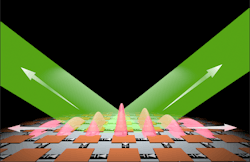
Until now, research into the photonic version of time crystals centered on bulk materials or 3D structures. Working on 3D structures is incredibly difficult, so the team wondered if a different approach might work: reducing the dimensionality from a 3D structure to 2D.
“Such a property would accelerate their design and implementation in realistic applications,” says Asadchy.
Photonic time crystals “may pave the way for the next generation of mirrorless lasers,” says Xuchen Wang, currently a postdoctoral researcher at KIT. “But the concept of photonic time crystals is still in its infancy and currently limited to bulk media, so achieving them posed a significant challenge and required further investigation.”
Creating a 2D photonic time crystal
The team’s 2D photonic time crystal approach worked—and they designed and synthesized a 2D electromagnetic structure with embedded tunable components (see Fig. 3) to dynamically repeat its electromagnetic property in time.
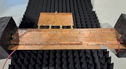
Their 2D electromagnetic structure, a.k.a. a metasurface, is ultrathin and was designed to work at microwave frequencies for a proof of concept. It’s composed of spatially periodic meta-atoms, and each meta-atom is periodically modulated in time by electronic varactors (a semiconductor diode with a capacitance dependent on applied voltage).
The main benefit of the team’s 2D photonic time crystal is that it’s essentially a skin-like metasurface, with the remarkable ability to act like a laser by amplifying incident light.
“In contrast to static materials, time-varying materials with properties that repeat in time are ‘non-Hermitian,’ resulting in a breakdown of energy conservation,” says Wang. “As a result, when light is shed into such materials, it’s possible for amplification to occur. This is the underlying physical principle behind photonic time crystals.”
The team experimentally verified theoretical predictions about their 2D photonic time crystal’s behavior and observed strong wave amplification. “I was thrilled when I turned the time modulation button ‘on’ in the lab and saw that the microwave power was amplified by more than 100 times,” Wang says. “It dawned on me this was the first photonic time crystal that can be used in real-world applications.”
One of the biggest obstacles in this work was the design and experimental verification of the structure. “For instance, the microwave design process is a complex undertaking, requiring extensive knowledge in areas such as microwave wave circuitry and electromagnetics,” says Wang.
Beyond this, it’s necessary to consider numerous practical factors: the modulation speed of varactors and modulation strength, the operating frequency, and the fabrication limitation to ensure successful implementation.
“Remarkably, not only did we not lose in the functionality of photonic time crystals when we reduced the dimensionality, but obtained new features previously inaccessible with 3D photonic time crystals,” says Asadchy.
The most surprising aspect of this work is “it revealed that even 2D single-layer photonic time crystals can exhibit properties similar to their volumetric 3D counterparts, which is a highly surprising and exciting discovery,” says Wang.
Wide range of potential applications
2D photonic time crystals have an astounding range of potential applications. For starters, laser design can be simplified by removing the need for bulk mirrors typically used in laser cavities.
And 2D photonic time crystals not only have electromagnetic waves hitting them in free space, but waves traveling along the surface as well—and these surface waves can be used for on-chip communications between electronic components. When a surface wave propagates, it suffers material losses and its signal strength weakens. Integrating 2D photonic time crystals into the system enables the surface wave to amplified so communications are efficiently enhanced.
Since they amplify electromagnetic waves, 2D photonic time crystals can also make wireless transmitters and transceivers more powerful and efficient. Want to prevent signal decay (a significant problem in wireless transmission)? Coating surfaces with 2D photonic time crystals may provide a solution.
2D photonic time crystals also show potential for being integrated into future reconfigurable intelligent surfaces at microwave- and millimeter-wave frequencies, such as those within the upcoming 6G band, to enhance wireless communication efficiency. “The idea of using 2D photonic time crystals can potentially be applied to the optical band as well, which would reduce the difficulty of using them within this band,” Wang says.
Since the team has already verified the concept in microwave frequencies, their next step is “to explore the possibilities of building a 2D photonic time crystal in optics and the benefits it may offer,” he adds. “By shifting our focus to optical frequencies, we hope to uncover new insights and opportunities that can shape the future of this technology.”
Timeline to use? The microwave 2D photonic time crystals “can be readily integrated into modern 6G reconfigurable intelligent surfaces to enhance communication efficiency by directly amplifying the electromagnetic waves,” says Wang. “Optical designs can certainly be challenging and time-consuming to develop, so it’s still difficult to predict when it can be used.”
FURTHER READING
X. Wang et al., Sci. Adv., 9, 14 (Apr. 5, 2023); doi:10.1126/sciadv.adg7541.
Related Article
About the Author

Sally Cole Johnson
Editor in Chief
Sally Cole Johnson is Laser Focus World’s editor in chief, and she has more than 25 years’ experience as a science and technology journalist. She specializes in physics and semiconductors, and wrote for the American Institute of Physics for more than 15 years, and also covered theoretical physics and neuroscience for the Kavli Foundation, and complexity for the Santa Fe Institute. Johnson has also written extensively about military embedded systems, high-performance computing, software-defined networks, and infosec. She is a member of the National Association of Science Writers (since 2001).
When she isn’t writing about optics, photonics, or quantum advances, you can find her outside in northern NH in the garden with birds landing in her hand or heading for the mountains with her bike, skis, or crampons and ice axe.