A team from the Australian Research Council Center of Excellence for Transformative Meta-Optical Systems (TMOS) has made a breakthrough in 3D dynamic hologram technology.
The technique uses meta-optics (metasurface optics)—flat lens technology that can manipulate and transform light with unprecedented accuracy. It involves fabricating microring-shaped laser cavities out of indium phosphide (InP), a semiconductor material, using a crystal growth technique called selective area epitaxy (see video).1
Semiconductor nanowires are common types of nanolaser cavities, says Wei Wen Wong, a research officer at Australian National University and lead author of the work. But while nanowires offer advantages such as strong confinement of light and a small device footprint, integrating vertical nanowires as nanoscale light emitters directly on a device is challenging, mainly because photons leak at the base of the vertically standing nanowire cavities.
Ring-shaped laser cavities also possess poor emission directionality, the researchers note, causing photons to scatter in multiple directions. This is a problem because hologram devices require highly directional light beams.
The researchers’ approach overcomes these hurdles. “When the microring cavities lase, most of the photons travel in a direction parallel to the bottom substrate, which effectively reduces photon leakage,” Wong says.
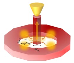
Their technique combines advantages of both the microring and nanowire cavities. By coupling the laser emission from the microring laser into a vertical nanowire at the center of the ring cavity, photons can be emitted at the top surface of the nanowire. Nanowire cavities can be designed to emit light with much better directionality.
The microring laser is much more efficient than the nanowire, and essentially acts as the system’s light source; the nanowire cavity functions as a highly directional nanoantenna (see Fig. 1). “This configuration allows us to shape the laser beam in a specific way,” Wong says.
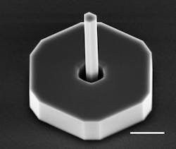
The entire system was developed via a “bottom-up approach,” which means no etching or mirror polishing are needed. These steps are often required in conventional semiconductor laser fabrication.
“The entire system is ‘grown’ from scratch on the device substrate,” he says (see Fig. 2). “Post-growth etching often roughens the sidewalls of laser cavities, which degrades device performance. It is very challenging—practically impossible—to fabricate our system with any conventional fabrication approaches.”Most of the reported outcoupling methods involve some sort of deformation of the shape of the ring cavity, which can degrade device performance and lasing efficiency. Without any post-growth fabrication steps on the grown cavity structures, the researchers were able to couple the photons out toward the vertical direction (out-of-plane). They discovered this is very useful for display applications such as emitters for hologram devices.
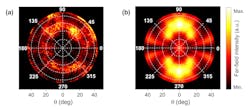
The researchers are now working toward fabricating arrays of coherent, miniaturized light emitters with tunable emission directionality and beam shape (see Fig. 3). Each array could potentially function as an individual, addressable, and tunable pixel in the hologram device, projecting 3D images in free space.“3D hologram devices can potentially find some very critical applications in the medical field,” Wong says. “For instance, a hologram device that can project real-time 3D images of a patient’s organs can be very helpful for surgeons and potentially improve the success rate of complicated surgeries.”
The meta-optic-based system is just 5 µm in size—unlike bulky, expensive systems that have hampered past efforts to develop hologram technology and make it available for widespread use—it’s small enough to someday be integrated into a portable tool that creates full-color dynamic holograms for doctors and surgeons, namely those who travel to remote areas where comprehensive healthcare can be difficult to provide.
Wong says next steps also include designing arrays of coupled ring/nanowire laser systems with controllable wavefront and achieving electrically injected lasing in these systems.
REFERENCE
1. W. W. Wong, N. Wang, C. Jagadish, and H. H. Tan, Laser Photon. Rev. (Dec. 18, 2022); https://doi.org/10.1002/lpor.202200658.
About the Author
Justine Murphy
Multimedia Director, Digital Infrastructure
Justine Murphy is the multimedia director for Endeavor Business Media's Digital Infrastructure Group. She is a multiple award-winning writer and editor with more 20 years of experience in newspaper publishing as well as public relations, marketing, and communications. For nearly 10 years, she has covered all facets of the optics and photonics industry as an editor, writer, web news anchor, and podcast host for an internationally reaching magazine publishing company. Her work has earned accolades from the New England Press Association as well as the SIIA/Jesse H. Neal Awards. She received a B.A. from the Massachusetts College of Liberal Arts.


