Terahertz photonic circuits possible with active and passive components
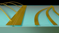
An integrated photonic platform recently developed by ETH Zurich researchers at the Institute for Quantum Electronics, led by Urban Senica, a Ph.D. student, and Giacomo Scalari, a physics professor, makes it possible to fabricate complex terahertz photonic circuits with both active and passive components (see Fig. 1 and video)—such as coherent comb sources, passive waveguides, reflectors, out-couplers, amplitude and phase control elements, and more.
Integrating mid-infrared and terahertz photonics is important for telecommunications and sensing, and one promising source integration candidate is the terahertz quantum cascade laser.
Recent advances in high-temperature operation of terahertz quantum cascade lasers, their agility, and the possibility of acting as frequency combs and high-speed detectors make them ideal building blocks for terahertz photonics.
“We work at terahertz frequencies, typically around 3 THz, which lie halfway between visible light and microwave frequencies,” says Senica. “This allows us to borrow and extend concepts from various parts of the electromagnetic spectrum into our devices. For this platform, we were inspired by the rich component gallery of integrated silicon photonics, where various components are integrated onto the same photonic chip. Our platform’s versatility means we’re now really limited only by our imagination.”
Terahertz quantum cascade lasers are typically fabricated on chips from wafers grown by molecular beam epitaxy. Following a complex fabrication procedure within a cleanroom, individual lasers (typically simple ridge waveguides consisting of active material) are produced. “These are excellent compact sources of coherent terahertz radiation, but often need to be used in combination with more complex external components and setups,” Senica says.
Planarized double metal waveguides and a low-loss polymer
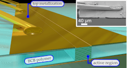
The team’s work centers on a high-performance planarized double metal waveguide with an extended top metallization. They improved the performance and extended the functionality of their fabricated photonic chips by using a low-loss polymer (Benzocyclobuten; BCB) on the sides of active waveguides, which results in a planarized geometry similar to other complex integrated photonics platforms.
Placing bonding wires on the extended top metallization over the BCB-covered area on the sides prevents the formation of any defects or local hotspots on top of the active region (see Fig. 2). This enables fabrication of a very narrow waveguide width that can be used as an efficient selection mechanism for the fundamental transversal lasing mode and is also beneficial for heat dissipation and high-temperature continuous-wave operation. The extended contact enables lateral heat flow, which improves the maximum operating temperature of the planarized devices.“Besides improving the laser performance in several crucial figures of merit, it allows us to co-integrate active and passive waveguide components on the same photonic chip,” says Senica.
Initially, the team was surprised by how big an impact their new planarized geometry had on improving laser and frequency comb performance—it significantly improves dispersion, RF, and thermal properties.
In terms of challenges involved, “the new fabrication process involves quite a few new steps of increased complexity, so optimizing each process step was really crucial to get the final excellent performance,” he notes.
One remaining challenge is the low operating temperature of terahertz quantum cascade lasers in general, because devices in the team’s work are compatible with liquid nitrogen operating temperatures (77 K and above). “But our field is progressing rapidly, with the recent demonstration of the terahertz quantum cascade laser devices operating on thermoelectric coolers, so we’re hopefully not far from room temperature operation,” Senica says.
As far as applications, the team’s devices may be used for coherent communications, spectroscopy, sensing, and imaging.
In their first demonstration, they focused on showing the basic functionalities and advantages of their integrated terahertz photonics platform. “We’re currently working on several new devices using our planarized waveguide geometry that will bring new concepts and functionalities to the terahertz frequency range,” says Senica. “And we’re very much looking forward to sharing our new results with the broader photonics community.”
FURTHER READING
U. Senica et al., Light Sci. Appl., 11, 347 (2022); https://doi.org/10.1038/s41377-022-01058-2.
About the Author
Sally Cole Johnson
Editor in Chief
Sally Cole Johnson, Laser Focus World’s editor in chief, is a science and technology journalist who specializes in physics and semiconductors.


