Dielectric nanocavity concentrates light in volume 12X below diffraction limit
A widespread misconception that it’s impossible to compress light below the diffraction limit in dielectric materials, which don’t absorb light and are widely used by the semiconductor industry, was refuted theoretically back in 2006. A group of Technical University of Denmark (DTU) researchers, led by Søren Stobbe, recently confirmed it by designing and building a bowtie-shaped dielectric nanocavity that concentrates light in a volume 12X below the diffraction limit.
The diffraction limit is a fundamental limit of imaging systems, such as conventional microscopes, but there is no such thing as a diffraction limit for dielectric nanocavities.
How did they pull off the feat of building the dielectric nanocavity? The group programmed their knowledge of real photonic nanotechnology and its current limitations into a computer, asked it to find an optimal pattern to collect photons resulting in optical nanocavity design (a bowtie), which they then built.
“We were motivated by both fundamental research and applications. There are exciting prospects of being able to do experiments exploring and operating at fundamental limits to the light-matter interaction strength, but we were equally excited by perspectives for the new quantum devices and optical interconnects that may be realized using these cavities,” says Stobbe, an associate professor in DTU’s Department of Electrical and Photonics Engineering.
The group was also driven by the basic nanotechnological challenge of building such devices in the real world, which required a new approach to integrate design and nanofabrication, as well as pushing the limits of nanolithography for silicon photonics.
“In 2006, the first theoretical paper outlining this new type of cavity came from the group of Michal Lipson, now at Columbia University,” Stobbe adds. “More recent theoretical work by the group of Dirk Englund (MIT) discusses how these cavities may be used to enhance bulk optical nonlinearities to be effective at the single-photon level, an effect that has so far only been realized with quantum emitters. Another important source of inspiration was works by the groups of Steven Johnson (MIT), Jesper Mørk (DTU), and Ole Sigmund (DTU), which showed that topology optimization is particularly powerful for designing dielectric nanocavities. In fact, Mørk and Sigmund quickly became collaborators on the project.”
Dielectric optical nanocavities
Optical nanocavities work by “storing light for a long time and concentrating it into small volumes,” says Marcus Albrechtsen, a DTU Ph.D. student. “There have been vast improvements in the research to increase the quality (storage time) of cavities, but improvements to the cavity mode volume (concentration) had so far only been achieved using metals, which absorb light, which is a problem for many applications.”
One reason for exploring metallic nanocavities was the widespread misconception that cavities made in dielectric materials can’t focus light beneath the diffraction limit.
“Rather than metals, we’re working on bowtie-shaped cavities made of silicon, and the cavity volume depends on the smallest possible feature that can be manufactured,” says Albrechtsen. “Since silicon is a dielectric material, absorption isn’t an issue.”
Their work centers on the integration of design and fabrication. “These are never entirely independent, of course, but our experiments required taking this integration to a new level: We directly measured the manufacturing tolerances of a state-of-the-art nanofabrication process, and then combined it with a state-of-the-art method for inverse design known as ‘topology optimization,’ to maximize the light-matter interaction inside silicon,” says Albrechtsen.
The result is a novel nanometer-scale cavity (see Fig. 1), which confines light 12X below the diffraction limit, where all features of the design can be accurately fabricated and the optical measurements confirm the numerical calculations.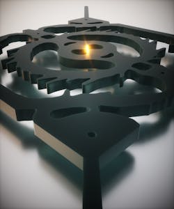
“While experimentally showing that dielectric cavities can confine light deep below the diffraction limit has a big impact across a number of applications, the underlying method of including measured fabrication constraints directly in the inverse design algorithm is also demonstrated in our work for the first time, and the same method can be used across a large number of fields from structural engineering to other chip-scale devices,” says Albrechtsen.
All features of the design are fully emergent from the topology optimization (see Fig. 2), the underlying physics, and the fabrication constraints.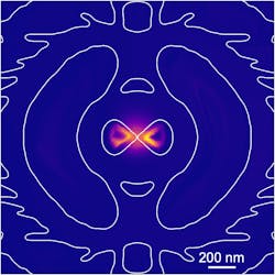
“All parts of the design serve a purpose, which can be understood in hindsight looking at the design, but the design would have been hard to come up with by relying on intuition only,” he says. “This includes both the bowtie feature and all of its ‘hairy’ features. Since manufacturing tolerances were taken into account, these aren’t just fancy additions but actual, maybe surprising, improvements.”
Previous work focused on optimizing the quality factor of cavities, which required fabricating smooth surfaces and reducing disorder. “But the mode volume directly depends on the size of the central bowtie feature,” explains Albrechtsen, “which marks a change in paradigm and focus for fabrication.”
A key challenge was to develop nanofabrication methods beyond the current state-of-the-art. “The 8 nm bowtie (see Fig. 3) we designed and fabricated using top-down fabrication is much smaller than conventional quantum light emitters, such as a typical quantum dot,” he adds.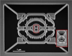
Surprises along the way
While the team’s work builds upon theoretical ideas dating back at least 16 years, many within the physics and nanophotonics communities still believe the optical mode volume in nanocavities is bound by the diffraction limit—unless it involves using plasmonic effects in metal nanocavities.
“Our experiments are directly showing—for the first time—mode volumes below the diffraction limit in a purely dielectric cavity,” says Stobbe. “Many nanophotonics researchers will be surprised these structures can even exist.”
Perhaps the coolest aspect of this work is the integration of topology optimization and nanofabrication, “because we feed measured fabrication constraints into the world’s most advanced algorithms for topology optimization,” he says. “It ensures resulting structures reach the strongest possible light-matter interaction, while at the same time are realistic.”
This integration of topology optimization and fabrication is demonstrated in the group’s work for the first time across any field of research and engineering. “Although the topology optimization involves too many degrees of freedom to ensure a global optimum, we have reasons to believe we are close and, in any case, our cavities are arguably the most highly optimized nanocavities ever built,” Stobbe says.
What’s next?
Early results open the door for new applications—including technologies to reduce the energy load of components within data centers, computers, and handheld devices—and experiments.
“An important research direction is integrating quantum emitters, which comes with its own set of challenges, because many common quantum emitters, such as quantum dots, are huge compared to the cavity,” says Stobbe.
Another key application is optical interconnects, which may significantly reduce the power consumption in integrated circuits by replacing lossy electrical wires with low-loss optical waveguides. “But this advantage can obviously only be harvested if the translation between the electrical and optical domains can be done with very high efficiency,” Stobbe says.
This, in turn, requires a strongly enhanced light-matter interaction, “and conventional cavity approaches don’t work because they either rely on high quality factors, which diminish the bandwidth, or absorbing metal cavities, which diminish the efficiency,” he adds. “In contrast, reducing the mode volume in a dielectric cavity increases the light-matter interaction without sacrificing bandwidth and without material absorption.”
Stobbe is looking forward to pushing the nanotechnology even further. “We’ve succeeded in confining light within 8 nm silicon bridges, and the question now is: How much smaller we can go? We’re working on some new concepts for self-assembly, which seem extremely promising and point toward atomic-scale silicon nanocavities,” he says.
FURTHER READING
M. Albrechtsen et al., Nat. Commun., 13, 6281 (2022); https://doi.org/10.1038/s41467-022-33874-w.
About the Author

Sally Cole Johnson
Editor in Chief
Sally Cole Johnson is Laser Focus World’s editor in chief, and she has more than 25 years’ experience as a science and technology journalist. She specializes in physics and semiconductors, and wrote for the American Institute of Physics for more than 15 years, and also covered theoretical physics and neuroscience for the Kavli Foundation, and complexity for the Santa Fe Institute. Johnson has also written extensively about military embedded systems, high-performance computing, software-defined networks, and infosec. She is a member of the National Association of Science Writers (since 2001).
When she isn’t writing about optics, photonics, or quantum advances, you can find her outside in northern NH in the garden with birds landing in her hand or heading for the mountains with her bike, skis, or crampons and ice axe.