Integrated photonics for quantum applications
In quantum computing, photonic quantum processors still lack the number of qubits compared to other types of quantum bits. But they hold promise, due to their potential in scaling up a photonic quantum processor.
For a fully functional optical quantum computer, photons must be generated, processed, and detected. Generation is achieved via a quantum light source that generates single photons that can be exploited to encrypt information. A combination of linear optics forms the necessary quantum gates where these quantum bits of information are processed. Finally, highly efficient single-photon detectors detect these photons reading the information.
What is magical about quantum photonic computing is that all of these building blocks can be implemented into photonic integrated circuits (PICs). Different promising platforms can serve the processes above, such as silica-on-insulator (SiO2), silicon-on-insulator (Si), silicon nitride (Si3Na4), lithium niobate (LN), gallium arsenide (GaAs), indium phosphide (InP), and others. Inevitably, the properties of each platform are different; each offers different desired features. Innovative solutions that allow the combination of these platforms into hybrid PICs are needed. In the near future, we will see the rise of hybrid platforms that combine different photonic technologies into a single functional unit, managing to overcome the limitations of monolithic photonic circuits.
Integrated single-photon sources
Generation of a single photon and its states on a chip are essential for all photonic-based quantum applications. Notably, by actively demultiplexing a stream of single photons into different spatial modes, it opens the door to the possibility of conducting quantum computing and advanced quantum sensing.
Quandela (Paris, France), a developer of quantum light sources and a photonic quantum computing solutions provider, works in this direction with their quantum dots, which are highly efficient sources of indistinguishable single photons. Quantum dots are “artificial atoms” fully integrated onto semiconductor materials, following standard semiconductor technologies.
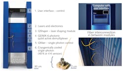
The company has brought this a step further with Prometheus, its first standalone quantum light source (see Fig. 1). The patented fiber-pigtailing technique allows for high integration in a plug-and-play 19-in. rack, which delivers high-quality photonic qubits for quantum information processing.
Sparrow Quantum (Copenhagen, Denmark) provides a single-photon source chip as a scalable solution for efficient photon generation based on a GaAs platform with InAs quantum dots embedded in photonic crystal nanostructures. Precise control over the environment around the quantum dots has led to the world’s highest fidelity of single-photon generation, and enables multiphoton interactions. The next step for Sparrow Quantum is to develop a user-friendly single-photon source that enables a plug-and-play experience.
Integrated single-photon detectors
On-chip detection of single photons allows the ultimate readout of quantum information. Several single-photon detector technologies are available, such as avalanche photodiodes and superconducting nanowire single-photon detectors (SNSPDs).
Pixel Photonics (Münster, Germany) has developed an approach for integrating SNSPDs onto a nanophotonic waveguide. Agnostic to the waveguiding material, the technology allows for integrating highly parallelized, efficient, and ultrafast single-photon detection with the preferred quantum photonic platform for the respective application. The detector geometry can be easily optimized for any desired wavelength, from the ultraviolet (UV) to approximately 2 µm. By combining passive (e.g., silicon nitride) or active (e.g., lithium niobate) quantum photonic components with the superior features of SNSPDs, Pixel Photonics’ technology is inherently suitable for wafer-scale manufacturing, enabling a new level of integration for quantum photonic applications wherever highly efficient single-photon detection is needed.
Integrated photonics for quantum communication
KETS Quantum’s (Bristol, U.K.) quantum security uses integrated photonics chips to allow flexible, cost-effective, and robust solutions to be deployed at scale, even in the most challenging environments. During the past five years, KETS has engaged with several chip organizations across various sectors, including telecommunications, governments, defense, and finance, to help them secure their systems and data with quantum-safe crypto solutions. Their technology miniaturizes quantum-safe hardware in a size, form-factor, and price point that allows it to scale for the quantum era.
KETS has worked with Airbus and other partners to successfully demonstrate quantum-safe communications between an unmanned aerial vehicle (UAV) and a ground station—a stepping stone toward satellite quantum key distribution (QKD).
Their chip-based platform provides a prototype solution under very challenging size, weight, and power (SWaP) constraints. They demonstrated the generation of secure keys with a gigahertz-operated transmitter over a high-loss free-space link (~25 dB) in daylight conditions.
In the telecommunications sector, KETS is the sole, new quantum encryption hardware supplier to ParisQCI, one of the first regional steps toward the larger, secure quantum communication infrastructure spanning the whole EU. To roll out this technology worldwide, the “Building a standardized quantum-safe networking architecture” (BaSQuaNa) project is a partnership between the U.K. and Canada, with the overall aim of developing the first transatlantic QKD communications network.
Data centers are essential facets of any data-driven world. KETS is co-leading a newly announced £11.6m Quantum Data Centre of the Future ISCF project. It will ultimately develop prototype integrations using KETS’ development kits as core building blocks and test and refine them into full applications with end-users.
Programmable quantum chips and photonics-based quantum processor
Photonic computing and processing occupy a leading position in the spectrum of so-called Beyond Moore approaches. The controlled manipulation of optical waves in amplitude, phase, and wavelength enabled by integrated photonics is a radical advancement of the established electronic digital computing paradigm using only electrons.
iPronics (Valencia, Spain) introduced the first programmable photonic processor with a broad range of applications, including 5/6G, communications, sensing, and computing (see Fig. 2). In relation to photonic computing, this technology explores optical interference to perform matrix-vector multiplications in an ultrafast and parallelized fashion. These features can be directly applied to quantum computation by incorporating single-photon lasers and photodetectors. This will allow the implementation of quantum logic gates, which are a key enabler of quantum computation. The programmability of these quantum gates is achieved through a user-friendly software platform, which unleashes the full potential of programmable photonics.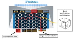
SiPhotonIC (Virum, Denmark) aims to bring fast and precise prototyping of quantum photonic integrated circuits (QPICs) both for commercial customers and research labs. The company designs and fabricates customized QPICs based on 220- and 250-nm silicon-on-insulator (SOI) technology. The platform was developed with low-loss photonic components tailored for quantum photonic applications. Depending on customers’ requirements, it relies on deep UV and electron beam lithographic processes, with delivery times of less than one to three months, making it very attractive for fast R&D iteration cycles that require a few SOI samples. Other materials and processes can be considered for custom QPIC projects. The company also offers on-demand additional backend services through third parties.
SiPhotonIC has a strong track record in manufacturing QPICs for well-known international research teams and companies that has led to publications in top-tier journals. Indicatively, generation or sampling of quantum states of light, quantum teleportation, quantum entanglement, QKD, error-protected qubits, and other quantum communication and quantum photonic computing concepts have been demonstrated with QPICs using SiPhotonIC’s SOI platform.
One of the most complex systems developed by SiPhotonIC is a single programmable QPIC designed for multidimensional quantum entanglement. A programmable photonic chip was fabricated to achieve this, integrating more than 550 photonic components onto a single chip, including 16 identical photon pair sources. The multidimensional system has demonstrated previously unexplored quantum applications, such as quantum randomness expansion and self-testing on multidimensional states.
SiPhotonIC expansion targets include releasing proprietary platforms based on state-of-the-art silicon nitride (SiN) and thin film lithium niobate (TFLN) technology for photonic prototyping for both quantum and classical applications, as well as for product developments. The company’s targeted applications include quantum photonic computing, quantum communications, and quantum sensing.
Highly flexible, low-loss photonic multichip integration
In a fully functional optical quantum computer, the aforementioned promising platforms to generate, process, and detect photons need to be incorporated. Vanguard Automation’s (Karlsruhe, Germany) photonic wire bonding and 3D-printed microlenses technology combines the complementary strengths of these different optical integration platforms in advanced photonic multichip modules, leading to compactness with high performance and great design flexibility necessary to reach the challenging requirements of a fully functional optical quantum computer. The technique relies on highly precise direct-write 3D laser lithography for printing of freeform single-mode waveguides between optical dies, thereby offering a path towards fully automatable photonic packaging up to mass production without the need for active alignment.
3D nanoprinting can also be used to fabricate facet-attached beam-shaping elements on optical chips and fibers, allowing for low-loss coupling with high alignment tolerance and for wafer-level probing of optical devices. The photonic wire bonds and 3D-printed microlenses have already demonstrated their capabilities in quantum applications (see Fig. 4).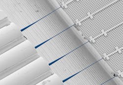
A second quantum revolution
Although much of this work is in a developmental stage, from the progress made to date, it is clear that we are entering a paradigm shift for quantum computing and quantum communication and on the verge of the second quantum revolution.
ACKNOWLEDGMENTS
EPIC wishes to acknowledge its members and collaborators who are always eager to share their ambitions and vision, particularly Diogo Costa and Anna Gonzalez, iPronics; Wladick Hartmann, Pixel Photonics; Caterina Taballione, QuiX Quantum; Stelios Pitris, SiPhotonIC; and Tom Crabtree, KETS Quantum.
About the Author

Panagiotis Vergyris
Dr. Panagiotis Vergyris is executive director at Specto Photonics (Milan, Italy). He has a Ph.D. in Quantum Photonics and more than 10 years’ experience in the photonics industry, with technical, managerial, and business roles in different deep-tech companies. Before joining Specto Photonics, he was a photonics program manager at the European Photonics Industry Consortium (EPIC), supporting startups in photonics, orchestrating successful business matches, and supporting and ensuring the viability of the European photonics ecosystem.