Optoelectronics packaging advance ruggedizes PNT devices for harsh environments
The U.S. military relies on assured positioning, navigation, and timing (PNT) devices for its everyday operations, as well as missions around the globe. And PNT devices are increasingly being used within harsh environments like space—where they experience high mechanical shock, vibrations, and huge temperature swings—or others with high humidity or dust.
This can lead to performance problems, because the way optoelectronics embedded within PNT devices are traditionally packaged and assembled isn’t suitable for harsh environments. It involves robotic alignment and bonding of several optical components and miniature mounts to a ceramic substrate, or bench, with gooey adhesives that tend to be sensitive to their environments.
To address this issue, Draper engineers, in Cambridge, MA, developed a new packaging and assembly method to ruggedize optoelectronics and reduce the complexity, labor requirements, and manufacturing costs.
The team’s advances in materials and methods for optoelectronic packaging “were driven by the continuing needs for smaller size, higher performance, increased ruggedization, and improved manufacturability for PNT solutions across a wide array of missions and platforms,” says Gilbert Feke, Draper’s senior member of technical staff, who works on photonics systems.
In many cases, “the key optical components central to PNT devices are quite unique and application-specific, such as wound fiber-optic coils used for interferometric fiber-optic gyroscopes (IFOGs) and the vapor cells for optical atomic clocks,” says Feke.
Draper and others have improved the design of these components as mission and platform needs to push further into harsh, highly dynamic environments. “But design and packaging of the general purpose componentry—such as lenses and beamsplitters—are equally important to the advancement of these PNT devices, because they must perform in concert with the esoteric componentry to achieve device operation with single-digit part per million or better precision within harsh environments,” he explains.
It’s well known, for example, that broadband multilayer dielectric beamsplitters “aren’t perfectly spectrally flat, but have residual spectral nonuniformity that’s dependent on the angle of reflection,” Feke adds. “Tiny changes in the angular alignment of the beamsplitter result in spectral shifts at the part-per-million level that results in a proportional measurement error.”
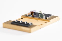
To address this challenge, the engineers turned to Draper’s in-house microfabrication facility to fabricate and optimize silicon optical benches (SiOBs). “SiOBs are wafer-level platforms composed of precision-etched surface features such as wet-etched v-grooves and pyramidal pits, and deep reactive-ion-etched (DRIE) slots,” says Feke.
These surface features efficiently and directly locate and integrate discrete microscale optical components without requiring additional mounts. “Our method enables multiple lenses and beamsplitters to be dropped onto the etched silicon topography, along with pieces of low-melting-temperature solid-glass frit, prefabricated into 3D shapes such as rectangular blocks and circular donuts,” Feke explains. “They’re designed to optimally register and anchor the optical components, and then simultaneously fused to the SiOBs during a single melt/cool step within a matter of minutes.” (See Fig. 1.)
Beyond this, they lithographically define v-grooves located with respect to the pyramidal pits whose purpose is to align the optical fiber assembled into the v-grooves with respect to the ball lenses assembled into the pits (see Fig. 2). “Our designs can accommodate both flat-polished fiber where the v-groove is centered with respect to the pyramidal pits so that the fiber is coaxial with the ball lens, as well as angle-polished fiber where the v-groove is slightly decentered with respect to the pit to account for refraction at the angle-polished surface,” he says.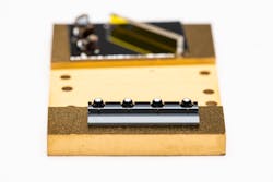
The new process replaces the time-consuming and high cost-of-ownership combination of precision robotics and liquid adhesives where the grabbing, releasing, and drifting of the optical components during adhesive curing is often problematic.
A die-attach challenge, and optical self-assembly
Silicon optical bench die must be pre-attached to a ceramic substrate prior to assembly of the optical components, so a significant challenge for the researchers was to develop a die-attach method—thermocompression bonding—that involves coating the materials with metal films and features. “This is followed by simultaneous application of heat and mechanical pressure to produce a metallurgical bond capable of withstanding the subsequent temperatures required for optical assembly,” says Feke.
One of the coolest aspects of this optoelectronics packaging work is the optical assembly method—it essentially self-assembles. “We could see under a microscope, once the starting materials were pre-positioned and then temperature cycled, the etched features within the silicon work in concert with the shapes and surface tension of the glass frit material to predictably force and then freeze the physical registration of the optical components to the etched silicon features,” he says.
Optimization of these etched features is critical. “For example, our technique involves mating the reflective face of the beamsplitter against one of the four sidewalls of a rectangular DRIE slot,” explains Feke. “While the simplistic approach to define such slots in silicon would be to lay out filled rectangular shapes in the photolithography layer, it results in sidewalls that aren’t perpendicular to the top surface of the silicon wafer but are slightly angled, which would skew the reflected beam out of plane. Instead of simple filled rectangular shapes, we etch rectangular outline features that confine unetched rectangular islands that drop out at the end of the process. By optimizing the width of the etched outline, we’re able to optimize the perpendicularity of the sidewalls of the resulting slots.”
This advance can be applied toward rapid prototyping of ruggedized PNT devices, where the concepts of rapid prototyping and ruggedization were previously contradictory. It may also decrease packaging costs and increase manufacturing scalability—both of which are important goals for the military.
“We’re looking forward to engaging with current and new customers to identify and execute on opportunities for our optoelectronic packaging capabilities,” says Feke.
About the Author

Sally Cole Johnson
Editor in Chief
Sally Cole Johnson is Laser Focus World’s editor in chief, and she has more than 25 years’ experience as a science and technology journalist. She specializes in physics and semiconductors, and wrote for the American Institute of Physics for more than 15 years, and also covered theoretical physics and neuroscience for the Kavli Foundation, and complexity for the Santa Fe Institute. Johnson has also written extensively about military embedded systems, high-performance computing, software-defined networks, and infosec. She is a member of the National Association of Science Writers (since 2001).
When she isn’t writing about optics, photonics, or quantum advances, you can find her outside in northern NH in the garden with birds landing in her hand or heading for the mountains with her bike, skis, or crampons and ice axe.