Unleashing the full potential of AI with in-package optical I/O
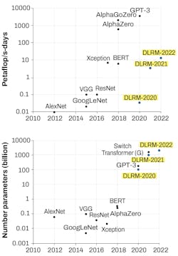
Today’s artificial intelligence (AI) models are growing in both size and sophistication at an unprecedented rate. Unfortunately, the traditional architectures found in data centers cannot satisfy the evolving demands of modern enterprise-level AI systems. An emerging solution is to use the composability capabilities provided by disaggregated system architectures. But the full potential of disaggregated architectures can be achieved only by means of advanced in-package optical input/output (I/O) technology.
Welcome to the second AI era
Although many people think of AI as being a relatively new development, it has been long in the making. Circa the 1840s, for example, while working with Charles Babbage on his Analytical Steam Engine, English mathematician and writer Ada Lovelace recognized that the numbers processed by the machine could be used as symbols to represent things like musical notes. In her writings, she noted that future machines “might compose elaborate and scientific pieces of music of any degree of complexity or extent.” Lovelace, who was the daughter of poet Lord Byron and mathematician Lady Byron, is considered to be the first computer programmer, and the modern computer language Ada is named in her honor.
The founding event of the field of AI as we know it today was the 1956 Dartmouth Workshop—more formally, the Dartmouth Summer Research Project on Artificial Intelligence. It was a seven-week brainstorming session between engineers and scientists, and it launched the first era of AI, which lasted to around 2012.
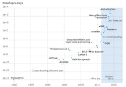
During this first era—as detailed in the AI and Compute paper from the AI research and deployment company OpenAI—there was a doubling of AI compute requirements approximately every two years, which roughly mapped onto the well-known Moore’s law.
Based on the development of new AI architectures and algorithms, 2012 was an inflection point in AI compute requirements across multiple domains: speech, vision, language, and games. This was the beginning of the current—second or modern—AI era, in which AI compute requirements are doubling approximately every three-and-a-half months (see Fig. 1).
Computation, however, is only one of the three main requirements demanded by enterprise-level AI. The others are access to vast amounts of memory and extreme data communication bandwidths. The former is provided by disaggregation and composability, while the latter can be addressed by in-package optical I/O.
Disaggregation and composability
A modern data center can contain hundreds or thousands of cabinets or frames called racks. Each rack can contain anywhere from 10 to 40+ bays or shelves. In a traditional architecture, each shelf contains a server and, in turn, each server features a motherboard containing one or more XPUs (CPUs, GPUs, FPGAs, ASICs), memory in the form of DDR DRAM modules, and storage in the form of solid-state drives (SSDs). In fact, there is a hierarchy of memory, because the latest generation of XPUs themselves may be presented as system-in-packages (SiPs) containing high-bandwidth memory (HBM) in the form of stacks of silicon dice.
Problems have emerged with this traditional architecture since computational workloads for tasks like AI and high-performance computing (HPC) have evolved to be larger, more complex, and more diverse than ever before. For example, some AI tasks may require thousands of GPUs and be GPU-centric, leaving CPUs and memory underutilized. Contrawise, other AI tasks may demand vast quantities of memory as compared to the number of XPUs, thereby leaving large numbers of CPUs and GPUs sitting idle.
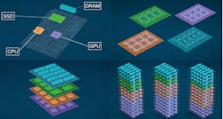
The solution is to use a disaggregated architecture, in which each shelf in the rack specializes in one type of component: CPUs, GPUs, RAMs, SSDs, which is referred to as “resource pooling.” (See Fig. 2.) Using this form of disaggregated architecture leads to the concept of composability, in which virtualized resources are automatically composed in near-real time to meet the computational and memory requirements of each task on an application-specific basis. Once an application has completed its task, its resources are released back into their respective pools, at which point they can be provisioned to future applications in different ratios.For disaggregation and composability to work, it is necessary for data to be able to pass from shelf to shelf and rack to rack at lightning speed with extremely low latency. Unfortunately, these bandwidth requirements far exceed the capabilities of traditional copper-based electrical interconnect technologies.
The solution is to use optical-based interconnects, but it is not sufficient to simply take existing devices (CPU, GPU, memory, etc.) and augment them with external optical interconnects. To achieve the necessary transmission speeds and bandwidths, the optical interconnect must be incorporated inside the device packages.
TeraPHY and SuperNova-based in-package optical I/O
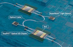
Fortunately, in-package optical I/O is now possible due to two recent developments from Ayar Labs in the form of TeraPHY optical I/O chiplets and SuperNova advanced light sources (see Fig. 4).Chiplets are small integrated circuits, each containing a well-defined subset of functionality. Multiple chiplets can be combined with the main silicon die by means of a base layer called an interposer or an organic substrate, with everything being presented as a single package to the outside world. By combining silicon photonics built on standard CMOS manufacturing processes, TeraPHY optical I/O chiplets allow the core device to communicate with the outside world at the speed of light.
Each TeraPHY chiplet supports eight optical fibers with eight channels per fiber. In turn, each of these channels currently supports a bandwidth of 32 gigabits per second (Gbit/s) with a roadmap to 112 Gbit/s. This means that each TeraPHY chiplet currently supports an aggregate bandwidth of 2 terabits per second (Tbit/s) with a roadmap to 8 Tbit/s.
The remaining piece of the puzzle is provided by the SuperNova laser light source. Prior to the development of SuperNova, laser light sources targeting similar applications tend to use lenses that result in bulky packages, low yields, and higher power consumption. By comparison, the use of patented microring photonic modulator technology means that each SuperNova is physically small and parsimonious in its power consumption, all while providing 8 wavelengths of light and driving up to 8 ports with a roadmap of 16 wavelengths driving 16 ports.
The combination of TeraPHY chiplets and SuperNova laser light sources is set to disrupt the traditional performance, cost, and efficiency curves of the semiconductor and computing industries by delivering up to 1000X bandwidth density improvements at one-tenth the power compared to traditional copper-based electrical interconnect technologies.
With optical I/O, it’s now possible for disaggregated racks of CPUs, GPUs, memory, and storage to be located tens, hundreds, or even thousands of meters from each other.
Increasing bandwidth through memory pooling with optical I/O
Many technologies will be able to take advantage of the extreme data bandwidths provided by in-package optical I/O. For example, Compute Express Link (CXL) is an open standard for high-speed connections between XPUs and memory. One CXL use model is that of memory pooling, in which many-to-many connections between hosts and devices are possible.
For example, a host can access all or part of the memory across multiple devices, while each device can act as multiple logical devices that are simultaneously accessible by multiple hosts. The capabilities of CXL will be dramatically enhanced by the addition of in-package optical I/O.
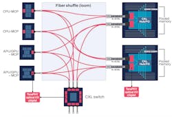
Figure 5 provides a conceptual visualization of a TeraPHY optical I/O chiplet providing increased bandwidth with shared pooled memory. This disaggregated solution enables direct, lower-latency access to DRAM for a collective of GPUs, as well as CPU and GPU access to common, shared, large-capacity memory. TeraPHY optical I/O chiplets allow seamless chassis and rack-scale scale-out between XPUs and pooled DRAM memory modules over CXL fabric as an example, with TeraPHY-enabled CXL switches expanding the scale-out to system-scale.The future is closer than you think
To satisfy the computational demands of cloud providers and data center owners, the world’s leading CPU and GPU companies are currently in the process of evaluating and adopting in-package optical I/O. In February 2022, for example, Hewlett Packard Enterprise (HPE) announced a multiyear strategic collaboration with Ayar Labs to usher in a new era of data-center innovation by developing silicon photonics solutions based on optical I/O technology. Similarly, in May 2022, Ayar Labs revealed it and NVIDIA are codeveloping groundbreaking AI infrastructure based on optical I/O technology to meet future demands of AI and HPC workloads.
Disaggregated architectures are shifting the paradigm of innovation by enabling resource composability for more efficient use of cloud and data-center resources. With the revolutionary ability to decouple memory from CPUs and GPUs, system architects can now allocate resources to match the unique requirements of individual workloads to improve application performance and reduce total cost of ownership.
Leading technology companies—including cloud providers and XPU manufacturers—are aligned regarding the need for next-generation disaggregated system architectures. Ayar Labs’ in-package optical I/O solution is the breakthrough needed to allow innovative, next-generation cloud and data-center disaggregated architectures to meet the exploding demands of AI and HPC workloads. Early adopters are planning on releasing products based on Ayar Labs’ revolutionary technology in 2023, with widespread deployment anticipated in 2024-2026.
ACKNOWLEDGMENT
TeraPHY and SuperNova are trademarks of Ayar Labs.
ADDITIONAL RESOURCES
- Unlocking the True Potential of AI with In-Package Optical I/O; see https://bit.ly/3y73qbL.
- Disaggregating System Architectures for Future HPC and AI Workloads; see https://bit.ly/3N6tqs0.
- Disaggregated System Architectures for Next-Generation HPC and AI Workloads; see https://bit.ly/3mQT0Xc.
About the Author
Uday Poosarla
Director and Head of Product, Ayar Labs
Uday Poosarla is the director and head of product for Ayar Labs (Santa Clara, CA).
