Optical filter coatings enhance communications systems
Optical thin-film filters are important building blocks of any modern optical communications system—they transmit a selected portion of the spectrum while rejecting other wavelengths. These components are generally made up of a multilayer stack of thin films deposited on a glass substrate. The working principle of an optical filter coating is based on optical interference theory.1,2
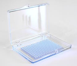
The design and manufacturing of the coatings determine the different filter functions of transmitting, reflecting, or blocking light in certain wavelength ranges. In some applications, such as wavelength division multiplexing (WDM), optical add-drop multiplexing (OADM), and passive optical networks (PON), the filter coating function follows the wavelength grid standards defined by the ITU or IEEE as well as other requirements, but the filter performance can be customized based on the specific needs. The typical size of a filter for optical communications is generally in the range of 1 to 3 mm. The filter is often coated on a large-size substrate or wafer and then processed into the final size. Figure 1 shows optical filter elements.
Optical thin-film filters were first used for telecommunications applications in the 1980s in early WDM systems, before the advent of optical amplifiers. With the development of optical amplifiers and transport systems in the early 1990s, dense wavelength division multiplexing (DWDM) gained interest from telecom carriers. Since then, thin-film technology has been the dominant filter technology that combines or splits optical signals or bands, to properly shape the optical spectrum, and to insert or extract optical channels into or from a transmission link. Its success in the market is due to its low cost, low loss, and temperature stability compared with arrayed waveguide grating (AWG) or fiber Bragg grating (FBG) technologies. In the early 2000s, DWDM 50/100/200 GHz filters and skip filters were successfully deployed in the fiber-optic telecommunications infrastructure.3
During the past 20 years, new types of filters have emerged due to the development of new standards, including coarse wavelength division multiplexing (CWDM), local area network wavelength division multiplexing (LAN-WDM), and shortwave wavelength division multiplexing (SWDM). New and very challenging filter designs such as dual-band and multi-band designs were developed to support these new standards. These designs reduced the number of filters in a packaged device, decreasing the insertion loss and making the overall device smaller. After the success of DWDM/CWDM/PON filters in telecom networks, filters became increasingly important for O-band CWDM, LAN-WDM, and SWDM transceivers deployed in datacenters.
Driven by the growing demand from datacom, the scale of filter production increased significantly, driving improvements in the deposition process, manufacturing control, and test automation, which resulted in considerable reduction in production cost. These technical advances enabled the widespread deployment of optical communications networks, which underpin the global internet.
From a technical point of view, a good optical filter coating process includes three main aspects:
Design for manufacturability. Generally, the optical thin-film coating design method is based on an initial stack, or so-called starting design. The numerical method is applied to refine the thickness of each coating layer to achieve the target performance. Selecting a good starting design is fundamental to achieving the required performance, and that is in large part dependent on the experience and expertise of the designer.
With the help of modern coating design software, it is not difficult to obtain a coating design that realizes very complex optical functions. However, when not supported by experience, this approach can result in designs that are not manufacturable in high volume. The most challenging and time-consuming task for filter designers is to arrive at the simplest filter design that will withstand the largest manufacturing process variability and still achieve high yield. Process variability can lead to errors in coating thickness and material refractive index. Sophisticated software simulation tools provide parameter details of manufacturing and monitoring processes, including deposition rate drifts, the rotation speeds of the substrates, the slit width of the optical monitoring system, shutter delays, and so on. Systematic and random errors must be distinguished and treated separately.4
High production efficiency. The selection of deposition processes often directly determines the batch cost of production. There are three main types of thin-film deposition processes for optical communications filters: ion-assisted deposition (IAD), ion-beam sputtering (IBS), and magnetron sputtering (MS). Among these, the cost of IAD is relatively lower, but the deposition rate fluctuations and inconsistency of the material refractive index across the coating limit its use in the production of the most complex filters, such as DWDM and gain-flattening filters. Compared to IAD, IBS and MS processes are capable of depositing films on relatively larger substrates. IBS is known to produce coatings of excellent optical quality with the lowest defect concentration. In comparison, the material deposition rate of MS is approximately double that of IBS, cutting the time for a single coating run by about a half.
Given the same deposition process and coating area, the yield (or effective coating area) determines the output and cost of the final filter product. The deposition process needs to be stable, repeatable, and well-controlled to achieve a high yield. All process settings and actual parameters, such as ion source, vacuum, gas flow, heater, and rotation speed, can be recorded and tracked to analyze the impact of fluctuations on the yield. Optimizing the yield means achieving the best coating thickness uniformity. For high-precision optical communications filters, the coating thickness uniformity error of the coated area needs to be controlled to within 0.07%.
Thickness control of complex coatings. Widely employed coating thickness control methods include time control, quartz crystal monitoring, and direct optical monitoring. Among them, the direct optical monitoring method can greatly improve wavelength targeting, which is critical for communications filters.
There are two types of optical filter coating stack structures. The first of such structures consists of quarter-wave (QW) layers, which are typically used to generate single-bandpass filters. The second type of structure is based on a coating stack, the layer thickness of which is fully optimized by the numerical method; there are no QW or “non-QW” layers after the optimization. For QW stacks, the coating system transitions to the growth of the next layer when the reflectance or transmittance intensity of the monitoring light signal reaches a maximum or a minimum. The optical thickness control based on this technique is called turning point monitoring. A great advantage of this real-time monitoring technique is that small errors in thin-film deposition can be corrected on the fly by adjusting the deposition of subsequent layers in real time.
For non-QW designs, an optical-level monitoring technique is often used to terminate each layer deposition when the light reflectance or transmittance intensity reaches a theoretically predicted level. For each non-QW design, an optical control strategy needs to be developed and implemented. Different optical-level monitoring strategies leverage different coating thickness prediction models, and there is no single, universal strategy suitable for all situations. The appropriate strategy depends on the deposition environment and the type of coating to be manufactured.
Mass-produced, high-end optical filter coatings
Although thin-film solutions for narrowband channel spacing down to 50 GHz and 25 GHz have been demonstrated, most of the market demand for DWDM filters is for applications at 100 GHz channel spacing. These 100 GHz filters are narrowband filters based on well-understood QW designs, which consist of five or six cavities. A six-cavity, 100-GHz filter provides steeper slopes (see Fig. 2). This translates into greater assembly tolerances of three-port packages.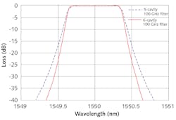
Beamsplitters are used to divide the incident light into two separate beams within a specified ratio. The angle of incidence of the coated surface is typically 45 degrees, leading to a perpendicular relationship between the transmitted and reflected light paths. One of the most important performance parameters of a beamsplitter is the maximum splitting difference between p and s polarization states of a uniformly polarized beam. Beamsplitters are available as cubes or plates. Plates are lighter and lower cost compared with cubes, but cubes can achieve the most uniform splitting difference between the p and s polarizations.
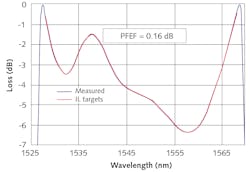
The design and manufacturing of coatings for beamsplitter cubes are quite different from GFFs and 100 GHz filters. First, the incident medium of the coating is glass rather than air. In the manufacturing workflow, the dielectric coating is applied to the hypotenuse of one of the two prisms; the two prisms are then cemented together to form a cubic shape. Moreover, one pair of high-index coating material and low-index coating material is not sufficient to achieve the desired nonpolarizing transmission. Typical designs involve at least three kinds of coating materials that are each carefully tuned. Figure 4 demonstrates the performance of a 50/50 non-polarizing beamsplitter coating design. This figure shows that three fully optimized coating materials can achieve less than 1% of polarization-splitting difference.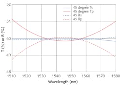
Optical filter technology has evolved, leveraging a long history of important achievements and thanks to years of technological progress in design and manufacturing tools. Coating optical filters remains a complex process that still requires expertise and experience to deliver the best performance with the highest yield. A deep understanding of the materials’ properties and deposition systems is the key to high-performance filter designs that will enable next-generation systems with higher spectral efficiency.
REFERENCES
1. A. Thelen, Design of Optical Interference Coatings (1989).
2. H. A. Macleod, Thin-Film Optical Filters, 4th Edition (2010).
3. R. B. Sargent and N. A. O’Brien, Optical Interference Coatings, OSA Technical Digest series, paper WA2 (2001).
4. A. V. Tikhonravov and M. K. Trubetskov, Appl. Opt., 44, 32, 6877–6884 (2005); doi.org/10.1364/ao.44.006877.