Silicon waveguides with material absorption of 13,000 dB/cm transmit well in the visible
Because silicon is transparent in the near-IR spectral region but quite opaque at visible wavelengths, silicon photonic circuits cannot ordinarily be made to operate in the visible region. However, Darius Urbonas, Rainer Mahrt, and Thilo Stöferle of IBM Research Europe–Zurich (Rüschlikon, Switzerland)—the same group of researchers who in 2019 created the world’s first ultrafast all-optical transistor capable of operating at room temperature—have experimentally achieved this feat, fabricating waveguides with losses down to 6 dB/cm in the 550–650 nm region in silicon, which has a material absorption of 13,000 dB/cm in this region. Their solution involves nanostructures, in the form of high-contrast gratings, with a striking behavior that some of the team members had already discovered over 10 years ago, albeit for another application.
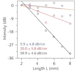
The high-contrast grating consists of nanometer-sized posts lined up to form a fence that prevents light from escaping. The posts are 150 nm in diameter and are spaced so that light passing through the posts interferes destructively with light passing between posts. Instead, most of the light gets reflected back inside the waveguide. The IBM researchers also showed that absorption of light inside the posts themselves is minimal. All this together translates to losses of only 13% along a light travel path of 1 mm inside the waveguide (see figure: blue = 600 nm, red = 700 nm, black = 655 nm, and orange = simulation at 600 nm). For comparison, in a pure silicon waveguide without the gratings, the losses would amount to 99.7% in a distance of only 10 μm.
Simulations showed that the grating would provide efficient broadband guiding of light over a broad band of wavelengths. Using a standard silicon-photonics fabrication process, the grating waveguides were fabricated; experiments confirmed low loss for visible light in the range between 550 and 650 nm. Simulations also show that this design may be used to make not only straight waveguides, but also to guide light around corners; however, the researchers have not yet experimentally confirmed this. Even if it proves feasible, some further optimization will be needed to keep the additional losses low in that case. A next step will be to engineer the efficient coupling of the light out of the waveguides into other components. That will be a crucial step in the team’s multiyear exploratory research project with the goal of integrating the all-optical transistors they demonstrated in 2019 into integrated circuits capable of performing simple logic operations. Reference: D. Urbonas, R. Mahrt, and T. Stöferle, Light Sci. Appl. (2021); https://doi.org/10.1038/s41377-020-00454-w.
About the Author
John Wallace
Senior Technical Editor (1998-2022)
John Wallace was with Laser Focus World for nearly 25 years, retiring in late June 2022. He obtained a bachelor's degree in mechanical engineering and physics at Rutgers University and a master's in optical engineering at the University of Rochester. Before becoming an editor, John worked as an engineer at RCA, Exxon, Eastman Kodak, and GCA Corporation.

